This thread has been locked.

If you have a related question, please click the "Ask a related question" button in the top right corner. The newly created question will be automatically linked to this question.

ADS8568: REFIO voltage of ADS8568 id abnormal

Part Number: ADS8568

Hello to whom it may concern


Our customer has problem that REFIO voltage is abnormal at ADS8568.

REFIO of normal device is 2.5V, but abnormal device is output 5V.


The power sequence at this time is as follows.


 (REFIO voltage is abnormal)

   #1 : ±12V(HVDD, HVSS)  -->  5V(AVDD)  -->  3.3V(DVDD)


However, when changing the power sequence to the following, the REFIO became correct voltage(2.5V).


   #2 : ±12V(HVDD, HVSS)  -->  5 V (AVDD)  -->  wait for power supply stabilization  -->  3.3 V (DVDD)

   #3 :  5V(AVDD) --> 3.3V(DVDD) --  >  ±12V(HVDD、HVSS)


In both sequence of # 2 or # 3, REFIO became normal.


(Question)

 1,  Does the REFIO be adversely affected  by the power supply sequence?

 2,  Which power sequence(#2 & #3) do you recommend as a measure to make REFIO normal?


Best regards,

Gk110

  • I may be having the same issue. Could someone at TI please answer this question.

  • Hello GK110,

    The reference circuit is related to AVDD, generally there are no specific requirements with regard to the power sequencing of the device. However, when HVDD is supplied before AVDD, the internal electrostatic discharge (ESD) structure conducts, increasing the HVDD current beyond the specified value until AVDD is applied, so it's better to power up AVDD earlier than HVDD/HVSS.  I have two questions:

    1.  For sequence #1, can the reference voltage be recovered to 2.5V after your power up sequence is done?

    2. Are you using hardware or software mode?

    Best regards

    Dale Li

  • Hello Gk110,

    Did you decide to go with sequence number #3? If so, does the REFIO always output 2.5V now?

    Also are you configuring the device through the serial port or through hardware?

    Thanks,
    Stephen

  • Hello Dale-san


    Firstly, I apologise for the delay in replying to you.


    > 1. For sequence #1, can the reference voltage be recovered to 2.5V after your power up sequence is done?


    The reference voltage be recovered to 2.5V when 3.3V power up with a little time after 5V(AVDD) was power up.

      It's #2 sequence.


      Also, when a phenomenon occurs, 2.5 V will be obtained even if 3.3 V power supply is turned OFF / ON.

      Furthermore, when a phenomenon occurs, 2.5 V will be obtained even if + 12 V power supply is turned OFF / ON.


      It does not recover with the reset signal.


    > 2. Are you using hardware or software mode?


     Our customer using hardware mode.


    Best regards,


    Gk110

  • Hello Stephen-san

    > Did you decide to go with sequence number #3? If so, does the REFIO always output 2.5V now?

    They don't decide sequence yet.
    Yes,#3 sequence always output 2.5V.

    > Also are you configuring the device through the serial port or through hardware?

    Sorry, I don't know.
    What can we know from the answers to this question?

    Best regards,

    Gk110
  • Hello GK110,
    Suggest to use option 3 and power up AVDD earlier than HVDD/HVSS even no specific sequencing requirement, however, when HVDD is supplied before AVDD, the internal electrostatic discharge (ESD) structure conducts, increasing the IHVDD beyond the specified value until AVDD is applied. Thanks.

    Best regards
    Dale
  • Hello Dale-san

    Thank you for your reply.
    My understanding is as following.

    1, When HVDD is supplied before AVDD, Is there it may cause REFIO voltage become incorrect?

    2, I understood that power sequence #3 is the best way to solve the problem.
     
    3, Although there is description that there is no sequence in the data sheet, since it may cause problems, I understood that there is actually a sequence.

    Is my understanding correct?
    Could you please reply?

    Best regards,

    Manabu Ito

  • Hello Manabu-san,

    Please give me few day to setup and do experiments to check.

    Thanks&Best regards

    Dale Li

  • Hello Manabu-san,

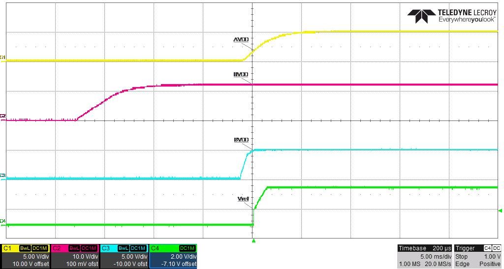
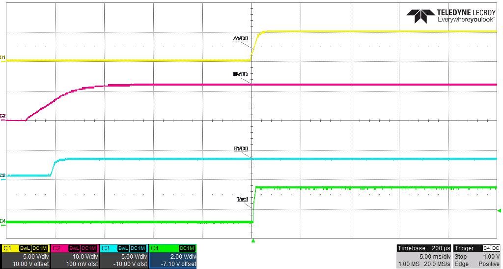
    After I did some experiments with ADS8568, the ADC worked well with different power sequences, the internal reference voltage is always correct, please check the screenshots from scope as below, AVDD is 5V, HVDD/HVSS IS +/-12V, BVDD(DVDD) is 5V, Green is internal voltage reference's output on REFIO pin. Thanks.

    Please pay attention to /STBY pin, this is an input pin and should be always connected to high for normal operation, I guess you have connected this pin to DVDD directly or by a pull up resistor. Please note that ADS8568 will be in standby mode for your connection on /STBY pin and it will not have a voltage output on REFIO pin until DVDD is available.

    Best regards

    Dale Li

  • Hello Dale-san

    Thanks for your work!
    I have a request to you.

    Could you please take waveform of power  sequence #3?

    Best regards,

    Manabu Ito

  • Hello Manabu-san,

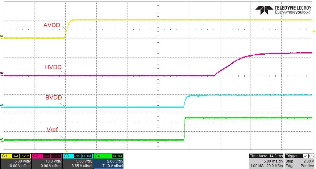
    This is the screenshot for #3 power sequence, internal voltage reference(Vref) is available when BVDD is available, and Vref voltage is correct 2.5V.  Thanks.

    Regards

    Dale Li

  • Hello Dale-san

    Thank you for your work!

    I'd like to confirm best solution.
    I'm going to suggest power sequence #3 to my customer.
    Is this suggestion a correct?

    Best regards,

    Manabu Ito

  • Hello Manabu-san,

    Based on your description, you can suggest #3, but I want to highlight two things to you:

    1.  Vref is related to AVDD, but Vref will be only available when BVDD is available if  /STBY pin is connected to BVDD directly or by a pull up resistor. 

    2.  Analog input voltage should be available later than HVDD/HVSS or at the same time, because Analog input voltage is limited between HVSS-0.3~HVDD+0.3V according to Absolute maximum Ratings table in datasheet.

    Thanks.

    Regards

    Dale

  • Hello Dale-san


    Thanks for your reply.


    I told about sequence with my customer.
    Then I received following question about sequence.

    (Question)
     If the sequence is below, is there any wrong?

     -12V(HVSS)  -->  5V(AVDD)  -->  3.3V(DVDD) --> +12V(HVDD)


     Best regards,
     

  • Hello Manabu-san,

    Generally, positive and negative power supply should be powered up together, based on your feedback, my recommendation is :

    5V(AVDD) --> 3.3V(DVDD) --  >  ±12V(HVDD、HVSS)

    Thanks.

    Best regards

    Dale