This thread has been locked.

If you have a related question, please click the "Ask a related question" button in the top right corner. The newly created question will be automatically linked to this question.

ADS1194: Chip does not respond to RREG command

Part Number: ADS1194

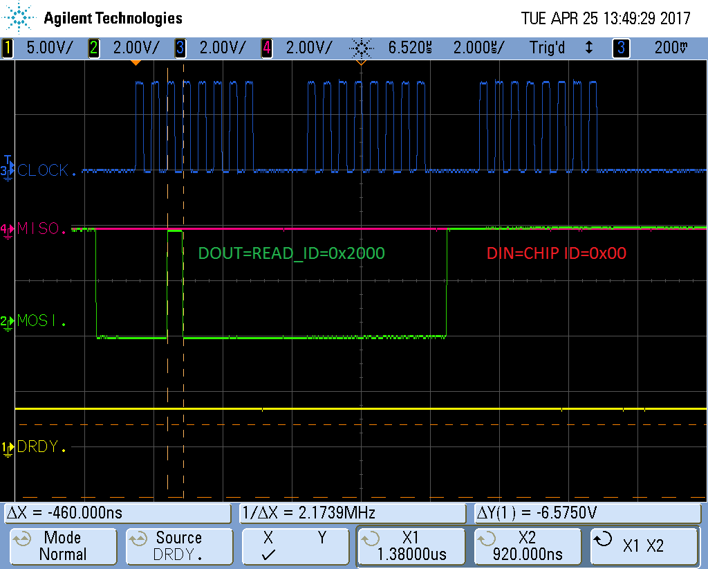
I have resetted my ADS1194 and sent a SDATAC command, after that I send a RREG(ID) command, but I don't get any response from ADS1194 which should be 0xB4. Attached is the oscop shot. Can you please help me debug this?( MOSI is DIN, MISO is DOUT)

  • Hello Arash,

    it looks like you are sending the correct instruction. One thing I can see is that the time between the bytes looks like it is close to or less than tsdecode specified on page 12. This is the time it takes the ADS1194 to decode a command that it receives. For example, if it receives 0x20, it needs 4 tclk to determine that you would like to read register 0. Then, after you send 0x00, it needs 4 tclk to determine that you would like it to shift out only 1 register. That time 4tclk comes out to a little less than 2 us using the internal oscillator. You should try to have the time between SCLK packets be greater than or equal to 2 us for RREG and WREG command (since they both require multiple bytes).

    Also, it is not pictured here, but please make sure chip select is held low for the entire transaction and does not pulse high in between the bytes.

    Regards,
    Brian
  • Hi Brian,

    Thanks for detailed reply. I think timing requirements are being met. Because 4xtclk=2us is from the end of first byte, to the end of second byte, which here is rouhly 5us. I also checked the CS and that's always low. I thought maybe my SPI read() is not correct, but as you see from the picture after sending the second byte, 8 clocks are being issues but ADS does not shift anything during that period. So problem should be in ADS I think.

    If I send a random value to ADS, does it drive the ADS to a nonfunctional state?

  • Hi Brian,
    After some testing, I could receive the Chip ID, but that happens only if I go to debug mode and run program step by step. If I let the program run at by its own, it doesn't recognize commands. So I am confused because as I explained in above, the timing requirement is being met(5us). So the chip should be able to respond. Am I missing something?
  • Hello Arash,

    Perhaps I'm reading the image wrong, but it seems like your time/div on the scope is set to 2us per div as shown in the upper right portion of the screen (the vertical grid lines are 2 us apart). If that is the case, it seems like the bytes are actually very close to 2 us.

    I actually think the fact that it provides the correct value in debug mode further validates this theory: having delays imposed in the routine gives the chip enough time to debug the commands.

    Perhaps try putting a little software delay between the bytes and see if that cleans it up.

    Regards,
    Brian Pisani
  • Thanks Brian. I put a little delay and it worked. But I think datasheet needs to be edited for multi byte part. In that section it's noted that SPI CLK<4MHz should be safe, and time between End of first byte to End of second byte should be >4.tclk, where in practice it the time between end of first byte and Start of second byte should be >4.tclk
  • Arash,

    I agree it is confusing since there are different requirements for different things. For example, when collecting data in RDATAC mode, there are no commands to decode so that requirement does not apply there. We will look into how to clarify things.

    Regards,
    Brian