This thread has been locked.

If you have a related question, please click the "Ask a related question" button in the top right corner. The newly created question will be automatically linked to this question.

ADS1248: device not entering "sleep" low power state with START pin low after conversion completes

Part Number: ADS1248
Other Parts Discussed in Thread: ADCPRO, ADS124S08EVM

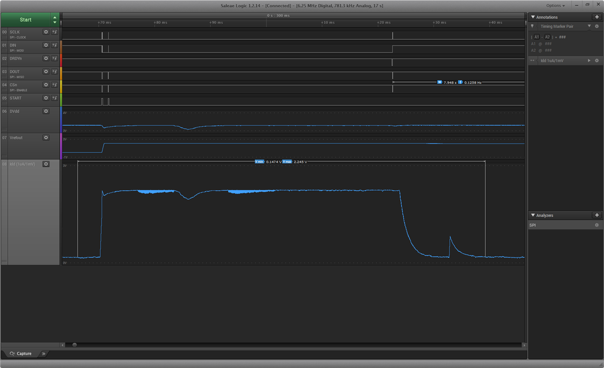
The device does not enter the "sleep" low power state when the conversion completes.  I see Idd = 174uA with START pin low.  Vrefout is disabled after the conversion completes.  The A/D is sampled every 8 seconds (first column below).  MOSI, MISO are the last two columns below

8.270505600000000,3,0x40,0x00
8.270511360000000,3,0x06,0x00
8.270517280000000,3,0x13,0x00
8.270523040000000,3,0x00,0x00
8.270528799999999,3,0x60,0x00
8.270534560000000,3,0x02,0x00
8.270540320000000,3,0xDD,0x00
8.270546080000001,3,0xFF,0x00
8.270551840000000,3,0xFF,0x00
8.270557600000000,3,0x4A,0x00
8.270563520000000,3,0x01,0x00
8.270569280000000,3,0x07,0x00
8.270575040000001,3,0x8C,0x00
8.271660960000000,4,0x04,0x00
8.271666720000001,4,0x04,0x00
8.322542720000000,5,0xFF,0x1C
8.322548480000000,5,0xFF,0x49
8.322554240000001,5,0xFF,0x12
16.270427680000001,6,0x40,0x00
16.270433440000001,6,0x06,0x00
16.270439199999998,6,0x13,0x00
16.270444959999999,6,0x00,0x00
16.270450719999999,6,0x60,0x00
16.270456480000000,6,0x02,0x00
16.270462240000001,6,0xDD,0x00
16.270468000000001,6,0xFF,0x00
16.270473920000001,6,0xFF,0x00
16.270479680000001,6,0x4A,0x00
16.270485440000002,6,0x01,0x00
16.270491199999999,6,0x07,0x00
16.270496959999999,6,0x8C,0x00
16.271582720000001,7,0x04,0x00
16.271588640000001,7,0x04,0x00
16.322463519999999,,0xFF,0x1C
16.322469280000000,,0xFF,0x49
16.322475040000000,,0xFF,0x2E

  • Richard,


    When the START pin goes low, the ADS1248 should complete the current conversion and then go to the low power state.

    My guess is that in your system, the internal reference is still on. In your system, I would check the VREFCON[1:0] bits in multiplexer control register 1. You can find the writeup on page 59 of the datasheet. The internal reference control for these bits may be set to 01, for which the internal reference is always on. If you set these bits to 10 or 11, the internal reference is on when there is a conversion in progress and turned off when the SLEEP command is issued or after the START pin is taken low.

    Just as a check, I measured the current of the device while converting at 5SPS, with a PGA=1. The AVDD current is 222uA (compared to the 225uA listed in the datasheet). When the internal reference is turned on, this current jumps to about 389uA.

    If I set the internal reference to be always on, and take the START pin low, the current drops to 168uA. The datasheet lists 180uA, while your measurement is 174uA. This is close to the current required for the internal reference, so my guess is that the internal reference is always on. If I set the reference to shutdown with the SLEEP command or the START pin transitioning low, then I see the current drop to 0uA.

    Again, check your reference settings. If this doesn't solve your problem. Let me know, and we'll think about other possibilities.


    Joseph Wu

  • Hi Joseph,

    I set register 2 to 0x60 (see above) and I do see Vrefout droop down between conversions. So I don't think it's the internal reference being on. I have Saleae Logic Analyzer captures and screen shots to upload if that helps. Other ideas?

    Thanks,
    Richard
  • Richard,


    I don't see anything that could be wrong at this point. You're right that it looks like the VREFOUT droops and shuts off after START goes low. Are you monitoring the current with a multimeter? Are you able to send any command to the device that shuts everything down? How much is your current when everything is on?

    I was able to open the Saleae file to look through the command set to see what you're doing. However I don't see anything that would cause an extra draw of current. I did have a few questions about the sequence.

    Looking at the logic analyzer, it looks like you set up the devices, issue a sync command and then wait for the data ready to read the data. It looks like you repeat the sequence 8 seconds later. Here's a close up of the WREG sequence:


    The sequence is 40 06 13 00 60 02 CC FF, then 4A 01 07 8C. In real terms, this is a WREG starting at 00, of 7 bytes, setting inputs to AIN2/AIN3, VBIAS off, reference on, but shutdown with SLEEP. CC FF FF written to the offset calibration register. Then there another WREG to the IDAC register for two bytes. This sets the IDAC magnitude to 1.5mA, and the outputs are IEXC1 and the other is disconnected.

    After that, you send 04 04 to SYNC the device, and then there is a read in about 50ms after the conversion completes. This repeats itself after 50ms.

    First, why do you have an offset calibration setting for CC FF FF? That seems like a very large negative offset. It won't change the current, but it is a bit unusualy large for the offset calibration.

    After the WREG commands, can you put in a RREG of the entire register map? I'd like to make sure that the device understood the WREG. There might be something else to see in the register map.

    Once you get the RREG, post another Saleae file, and I'll look it over.


    Joseph Wu

  • Richard,


    Also, are you able to post a schematic here? It might be helpful to see how you have your system connected and if there is any other possible current drawn from the supply. If you don't feel comfortable posting your schematic here, reply back and we'll figure another way for me to see the schematic.


    Joseph Wu
  • Hi Joseph,

    I'm not sure if I can share the schematics, but I'll check on it.  I have the ability to externally switch off the power to the A/D via S/W.  I measure the current with a "uCurrent Gold" https://www.eevblog.com/product/ucurrentgold/ with its output going into the Saleae A/D.  This is the bottom trace on the screenshot png.  The scale is 1mV/1uA.  I see a baseline additional current of ~ 147uA when the A/D is powered and has taken a reading but should be sleeping versus ~0uA when I switch off the power to the A/D via S/W after taking a reading.

  • Hi Joseph,

    I believe the offset calibration is not too big, -52 decimal?  It is the value the was obtained by doing a SELFOCAL.  I will attach a Saleae file that includes a register dump in addition to the standard 8s A/D sample.

    Thanks,

    Richard

    A2D_no_sleep_5_25_17A.7z

  • Richard,


    Sorry, you're right about the offset calibration. I'd forgotten that the offset calibration registers show the lsB first in the register map. FFFFCCh is fine for an offset calibration value.

    In the last post, you wrote 147uA instead of 174uA. It was 174uA, correct? It looks like you're measuring it from a small shunt resistor. Is the supply going only to the ADS1248? You don't have any front end conditioning or filtering that might draw current? Even a partial schematic would help.

    Give me a chance to look through the Saleae file. I'll see if there's anything in the register map that I have questions about.


    Joseph Wu
  • Richard,


    Sorry, I misuderstood what you said about the current. You said that during operation, the baseline was about 147uA higher. Does that mean that during operation, the current is about 321uA (147+174)? That strikes me as a bit low. What is the dc input voltage of AIN2 and AIN3 at the time? There is some variability in the current consumption when the input is larger because of the PGA, but I still would have expected the current to be larger than 380uA.


    Joseph Wu
  • Hi Joseph,

    No, not during operation. You are correct, that is way too low! From the PNG you can see operational current is 2.245mA (Vmax 2.245V) (A/D + our CPU). The 147uA is when the A/D should be asleep along with our CPU. That is what I call baseline. It should be only be 1uA or so but you can see it on the PNG at 147uA (Vmin 0.147V). If I turn off the power to the A/D via S/W, the baseline drops to 1uA. I measured the average current with an Fluke 89 IV meter and it agrees with the 147uA higher baseline current I see with the uCurrent Gold 10 ohm sense resistor and the Saleae.

    Thanks,
    Richard
  • Richard,


    I still don't see anything the Saleae file. It looks like the WREG has taken, and the read back of the regisiter map comes up ok. In the Saleae files that you send, it does look like the device has gone to sleep because you can see the VREFOUT lines go back to 0. Note that the files that I received, the VREFOUT is shown as a digital line (I'm guessing that the analog data would make the file to large to put into a post.

    You say that When you shut off the power through S/W (I assume you mean software), the current goes to 0V. How are you doing that? Is it through a switch connected to the GPIO of a microcontroller? Are you issuing a SLEEP command to the device? Is the digital supply connected to the same source?

    When you are operating the device you use the REF0 inputs for the reference. What is this connected to? Is this a for some sort of ratiometric measurement for an RTD?

    Also, if you use a shunt resistor of 10Ω and it drops 2.245V, you're really close to the min supply of 2.7V if you're running off of a 5V supply. Is there a reason you're not using the Fluke 89 as an ammeter to measure the current?


    Joseph Wu
  • Hi Joseph,

    Yes, it does seem like the A/D goes to sleep (Vrefout decaying down), but something is still consuming power in it... Yes, analog capture is ~600MByte.

    I use a IC-TPS27082L to switch the supply to the A/D via GPIO. I am not issuing a SLEEP command. Dvdd and Avdd are connected to the same switched supply.

    Yes, this is a 4 wire RTD with a 499 ohm resistor on Refp /Refn. All A/D readings are correct and accurate, only the excess current is the issue...

    I believe the drop in the 10 ohm resistor @ 2.245mA is only ~22mV, not an issue? The analog waveform "Idd (1uA/1mV)" is measuring current, not the supply voltage. The waveform above it measures Dvdd, and it stays well above 3.0V. I use the shunt and the Saleae A/D so that I can correlate my code with current consumption to help identify "bad actors" and minimize power consumption. I can integrate the current waveforms and check that average against the Fluke 89 IV.

    Would it be possible for you to try my register settings and see if you can reproduce my problem?

    Thanks,
    Richard
  • Richard,

    I was able to duplicate the setup, but didn't see any problems with the current. I used the ADS124S08EVM with ADCPro as the controlling software. It's not a perfect duplication of your setup, but it is very close. Here is the setup:

    You can see the ADS1248EVM on a breakout board in front of the MMB3 controller board. I use an Agilent 34401A for the current meter.

    With the software, I set the device to AIN2/AIN3 inputs, PGA1, 20SPS. The reference is on, but is shutdown when the device is shutdown. IDAC current is 1.5mA, where IDAC1 is set to IEXC1, and IDAC2 is disconnected.

    At startup, the current is about 198uA. When I turn the reference voltage on, current goes to 389uA. After I turn the IDACs on, the current goes to 517uA (note that the IDACs are not connected to anything at this point). Then I connect IEXT1 to AVSS to shunt the current and the current goes to 2mA.

    Using the START pin, I can pull it down to ground and the current returns to 0.1uA. When I pull up the START pin, it begins converting again and the current returns to original 2mA. I still don't see any extra current.

    I don't have total control over what I write to the ADC through the software. I can only do so much with ADCPro. However, I do grab some snapshots of the Saleae file. To show what is written to the registers of the device.

    Note that I use 40h in the MUX1 (02h). In your program, you use 60h in register. This should give the same result. If you want, you could try changing it, but the two bits that define the reference behavior are same.

    In your system, try measuring the current as you start up the device, and start to program the settings. If you can, try to match the currents in the datasheet. There might be some small variation in current because I didn't try to tie the inputs to mid-supply. This might cause the PGA (even in gain=1) to have some extra current load.

    joe wu

  • Hi Joe,

    Thanks for duplicating my setup and running this test.  This is quite helpful!  The fact that you have proven the same code and register settings works on you H/W allows me to focus on the H/W differences on my end what may be contributing to the excess current.  I'll let you know what I find...

    Thanks,

    Richard

  • Hi Joe,

    I got to the bottom of the excess current consumption. Your were correct, it had nothing to do with the ADS1248! My problem was that the ADS1248 shares the SPI bus with the debug port on a TI C2540 BLE radio. I didn't realize that the C2540 had internal pulldowns enabled on the SPI data pins. When the last bit sent to the ADS1248 was a one, it ended up drawing the excess current from the C2540's internal pulldown.

    Thanks for all your help!
    Richard
  • Richard,


    I'm glad that you were able to solve your problem. I thought there might be something else drawing current on your board.

    If you have any further questions, please feel free to post back.


    Joseph Wu