This thread has been locked.

If you have a related question, please click the "Ask a related question" button in the top right corner. The newly created question will be automatically linked to this question.

ADS8689: SPI - Sending READ command but getting zeros

Part Number: ADS8689

Dear All,

for a student competition we need to use fast and high-resolution ADCs to sample data with Arduinos. However, after reading through the ADS8689 datasheet several times and trying variuos commands, we were not able to get any reading from the device.

In order to check the data transmission I tried to read the ALARM_H_TH_REG Register to get FFh. So I send the following bytes after puling CS to low:

"01001000" (READ-command plus first bit of Address [48h], In the datasheet, table 5 it sais 01001_xx_<9-bit address>, thats why I added a zero the first byte... (correct ?))

"00100100" (Address for Alarm register [24h])

"00000000"

"00000000" (send zeros and simultaneously read incoming byte [00h])

Then I pull CS high again and wait for 500 milliseconds.

On the oscilloscope I see, that the MOSI bytes arrive, yet on the MISO there iss a byte during the first byte (READ) but zeros uring the next three bytes. So my reading is 00h.

Also, the MISO line doesnt go up after CS goes high. Is that usual? Are my commands incomplete?

Further Information:

The ADC is mounted on a propper evaluation board, layout as in the datasheet.

I have exchanged ADCs and Arduinos, so failure of device is probably not the problem.

The SPI clock is set to 8 MHz, I also tried 2 MHz.

The Reset pin is constantly high.

Can anyone  help or maybe has a sample code (any language)?

If you need more Information, just tell me :)

  • Linus,

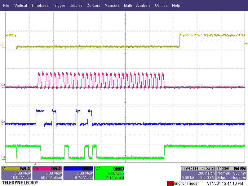
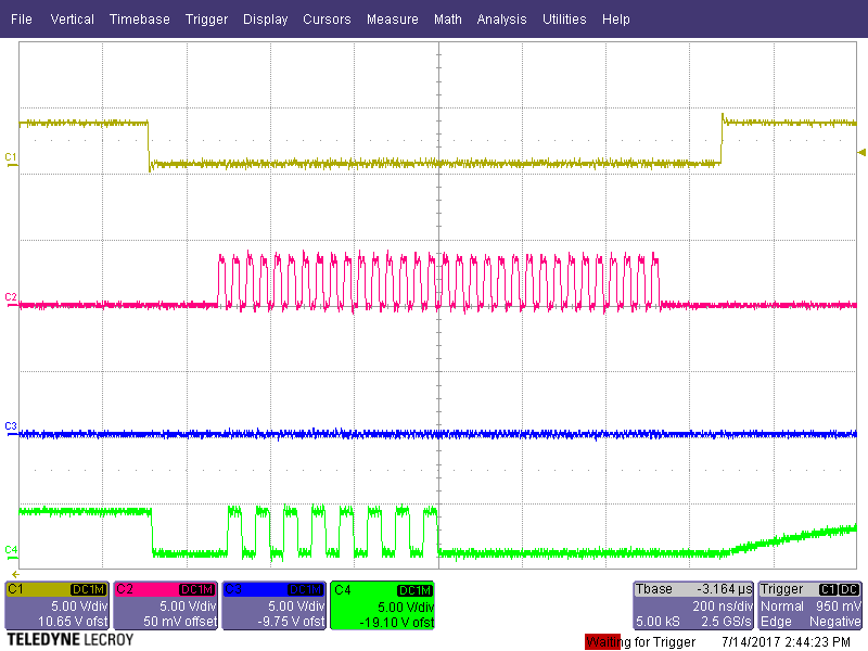
    Can you please attach a picture of the scope capture for SCLK, SDI, SDO, and CS? We can look at this to check for any timing violations.

    Best regards,
  • Hallo Art Kay,

    here it is:

    yellow is CS, blue is MOSI, red is MISO and green is the clock.

  • Linus,

    1. I think you are communicating correctly, and getting the expected results.

    2. The read command you are using is an 8 bit read. See page 54 in the data sheet. You may want to use the 16 bit read to get the full alarm threshold register. Now you are getting only 8 bits.

    3. The data can only be read in the next frame after issuing the read command (the 32 BIT transaction you show). So, if you repeat the command twice, you will see valid data on MISO corresponding to the register you selected in the first command.

    4. I believe that you have issued the command shown more than once, so you are reading the correct value for the ALARM_H_TH_REG here. The default for thisregister is FFFFh. So, you are reading the first byte of this register. If you used a 16 Bit read you could get the entire FFFFh.

    5. I suggest that you use write the register first and then read the device to confirm that you are getting back what you wrote.

    6. I suggest using the 16 bit write and read (READ_HWORD, and WRITE_HWORD). I think this will simplify your software as you will not have to do as many writes.

    7. The readback is the first byte in this example (FFh).  This is the readback for the previous frame.


    I hope this helps.

  • Hi,

    ok, I sent the following bytes now:

    CS low

    Writing:

    D0h    (Write two bytes command)

    24h    (Register address)

    55h    (alternating 0s and 1s)

    55h

    Reading:

    48h    (read two bytes command)

    24h    (Register address)

    00h    (send zeros and simultaneously read MISO)

    00h

    CS high

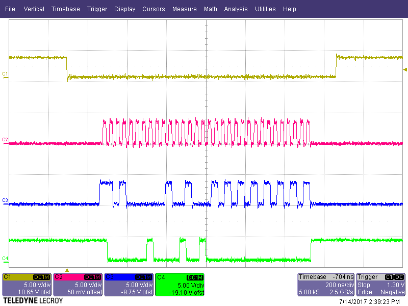
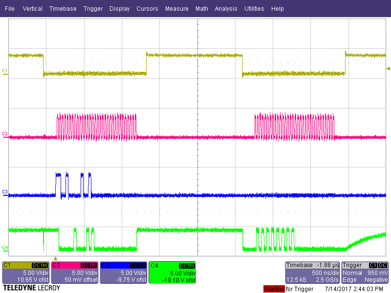
    The scope shows:

    Zoom on first 4 bytes (writing):

    Zoom on last 4 bytes (reading):

    My Arduino still reads zeros, although I wrote 5555h ...

  • Linus,

    1. I think your frame setup still has a small problem.  The frame should have 32 clocks in it.  I believe that you have 64 clocks in your frame.  You need to raise chip select (CS), between writing and reading.  I hope this solves your problem.
    2. Also, your digital signals have a lot of overshoot and undershoot.  This could be interpreted as data if it is bad enough.
      1. How is your board layout?  Did you create a PCB?  Do you have a good ground plane?
      2. Is your scope probe close to the digital pin’s you are measuring?  Do you have a good ground connection on the scope probe?
      3. Assuming the overshoot is real, you may consider adding a small resistor 50 ohm in series with each data line.  See page 22 of the ADS8689 users guide for a schematic showing this (R26, R27, R28, R29).  This will soften the edges of your waveform and minimize overshoot. http://www.ti.com/lit/ug/sbau252/sbau252.pdf
      4. Ideally you would use an ADS8689 evaluation module to make your measurements.  This board was laid out carefully to optimize performance.  If you are doing your own layout you http://www.ti.com/tool/ads8681evm-pdk

     best regards,

  • 1. I forgot pulling CS high in between the frames, thanks. Unfortunately it won't solve the problem yet.

    This is what my scope shows now (I am sending ffffh in Write command now):

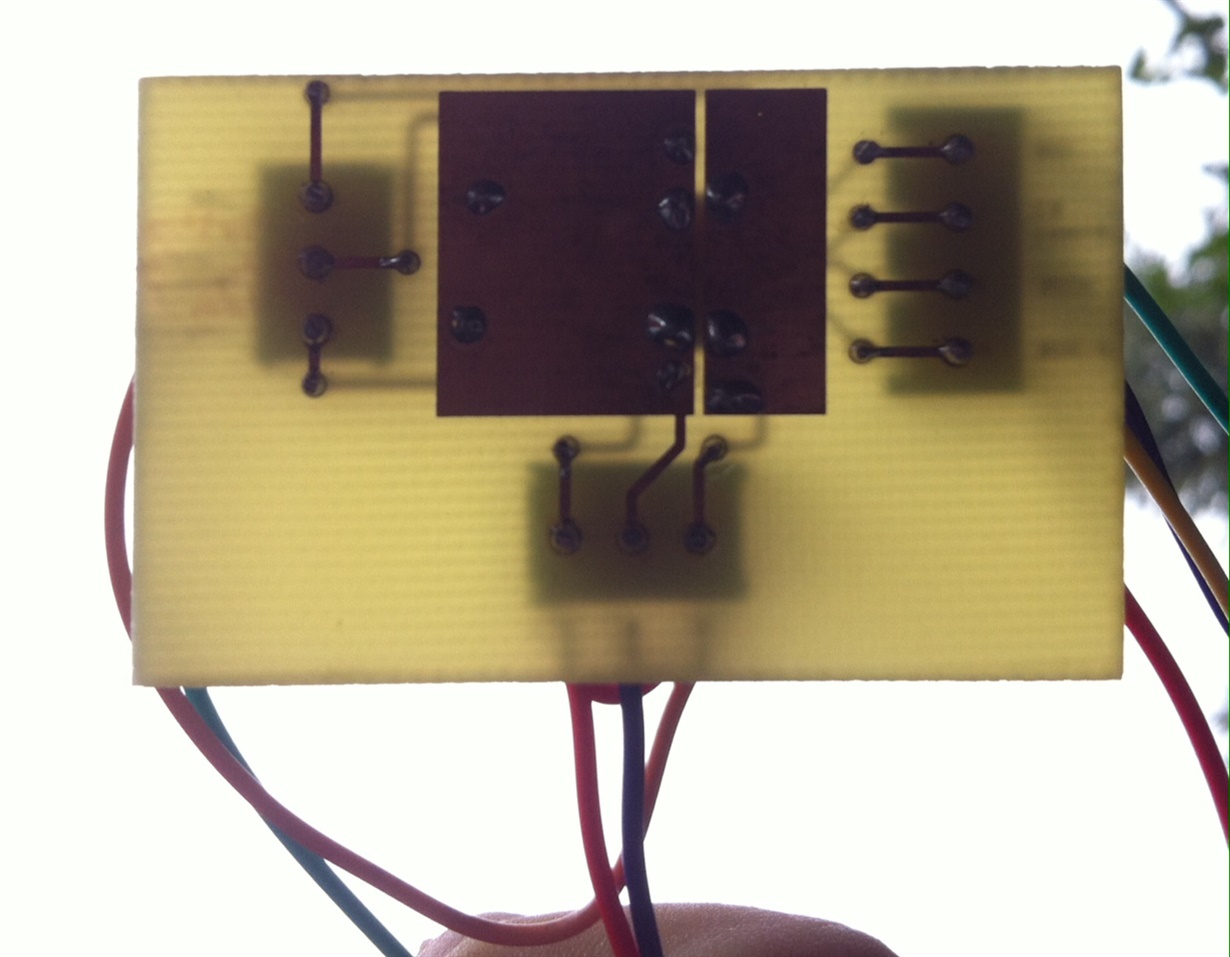
    2.1 The electronics workshop made a board for me, picture below. They followed the layout given by the datasheet.

    The lower pins are DVDD, GND and AVDD. The left ones are the 4 SPI pins. The right ones are RST (connected to DVDD, 5V) and Analog Input.

    I think the board layout should be fine.

    2.2 The scope is connected with 1m coaxial wires to the jumper wires of my setup.

    2.3 I tried the 50 Ohm resistors, they made the signals nicer

    2.4 If I cannot use the ADC like this, I would need to get the Eval, although it it quite expensive. And I thought it should be possible to do it on your own, but it seems to be a rather special ADC which is not made for single users but for massive industrial consumer.

  • Linus,

    I will get an evaluation module on my side and confirm the correct digital pattern.  This may take a few days as I have to get the hardware.

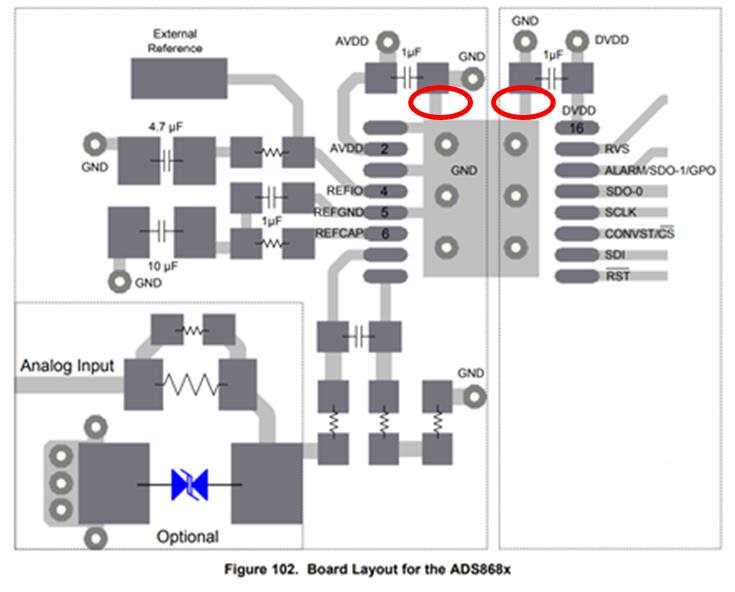
    If you followed the layout example in the data sheet the device should operate fine.  Looking at your layout, I do not see a top layer connection from the ground side of the capacitor to the ground plane under the capacitor (see circled below).   It looks like the capacitor ground is connected to the ground plane below with a via, but not to the top ground plane.

  • Hallo Art

    Thank you for your effort and committment to help me.

    Yes, it is true, the capacitors are not connected to the upper ground plate, but to the lower one. Can that be a problem?

    Backside of the board. The digital and analog ground are seperated.

  • Linus,

    Yes, you should connect the capacitors to the top ground plane. The inductance of via's can cause issues so it is best to have the power and ground on the top layer connect to the decoupling capacitor. This may not fix your communications issues, but will help with performance. The fix is easy, and you will not need a new PCB. Just place a small wire from the cap to the ground plane where the circles are in my previous post. Also, I will look into the actual device soon and give you more details on communications.

    best regards,
  • Linus,

    We have hardware now, so we should be able to confirm communications soon.

    best regards,
  • Hello Art Kay,

    ok great! I am looking forward to the results.

    Best regards

    Linus

  • Hi Linus,

    I have been working with Art on this and have captured both the write and read cycles on an oscilloscope (see below for photos of each cycle). Reviewing your second set of photos, I believe that two changes will allow you to read the specified register (a different read code and leave SDI low during the second frame of reading the register). Here is the step-by-step process:

    1) Pull chip select (CS) low and clock the hex code shown below into the ADC to write the value of 5555 to ALARM_H_TH_REG. When finished, release chip select.

    Hex code: D024 5555 (write 5555 to ALARM_H_TH_REG)

    2) To read the data back, two separate frames are required. In the first frame your host must provide the read command. To do so, pull CS low, clock in the hex code below (this is the READ_HWORD command, which will provide the full register contents), and release CS. Any activity on the SDO line is the last data conversion.

    Hex code: C824 0000 (read from ALARM_H_TH_REG)

    3) In the second frame needed to read the data pull CS low, provide 32 SCLK cycles and release CS. Do not change anything on the SDI line (leave it low). SDO will read back the value stored in the ALARM_H_TH_REG.

    Also, looking at your scope captures it appears that you might be getting noise between the digital lines. If the read value from the register is not what you expect, I’d recommend trying to clean up the signals. It may be as simple as ensuring that the spaces between the ADC’s pads are completely clean.

    Write cycle:

    Both frames of the read cycle (SDO in first frame is ADC conversion; second frame is register value)

    Read command (first frame of the read cycle)

    Read value of ALARM_H_TH_REG (note no activity on the SDI line)

    Hope this solves your problem, but let us know if it does not.

  • Hello Art and Evan

    I followed the instructions you gave me, the result is below in the oscilloscope. I am no longer reading zeros, but some randomly fluctuating value. The SPI signal is still very noisy, which might come from the arduino. For other SPI devices this was no problem, can it be in this case?

    overview (green=MOSI, purple=MISO, writing 0000h to register 24h, then reading register 24h):

    writing 0000h:

    reading:

    There are still some differences between our cycles due to the SPI library I use for the arduino:

    - my MOSI is usually high, yours is low

    - my MISO is usually low, yours is high

    - I have short breaks after every byte

    Is any of the above a problem? If not, then there should be something wrong with my layout or the ADC

  • Hi Linus,

    To clarify my previous post, a total of 3 complete frames are needed to write and read the register. Also, each frame requires 32 clocks, and CS must be kept low throughout the frame. Here is a summary:

    Frame 1) Write Command

    Drop CS and issue write command:

    D024 5555

    Raise CS

    Frame 2) Read Command

    Drop CS and issue read command:

    C824 0000

    Raise CS

    Frame 3) Read Register Value

    Drop CS, but do not provide any commands on the MOSI

    0000 0000

    Raise CS

    The register value is provided as the first 2 bytes of the third frame.

    Looking at the photos, make sure to keep CS low and provide 32 clocks when issuing the read command and add a 3rd frame to read the data. 

  • Oh, and I just realized:
    The MISO data does not change if I write a different value or write to another register. But if I put the Analog Input to ground or some voltage, MISO changes
  • Hi Evan,
    oh, yes I missread that. I will try that out.
  • Hi Linus,

    Regarding the MISO data not changing, that is to be expected. During the first two frames, this data will be the previous conversion. Thus until you change the analog input, the data should be the same.
  • Hi,

    as the SPI communication with the arduino library is not very useful, I now send the bites manually, which slows everything down as well.

    Unfortunately I still dont receive what I write to the register. The MISO does not seem to react on the MOSI. even if I send only zeros, I receive he same MISO.

    Do I still miss something?

    Below my scope (I pull the clock high before flipping CS, because otherwise the first clock pulses would have a smaller amplitude) :

    overview:

    Write frame:

    1st read frame:

    2nd read frame:

    If I send only zeros:

  • Hi Linus,

    It appears that in both read cycles there are 33 clocks. If that is the case, then the first clock of the 1st read frame (providing the read command) is clocking in a value of '0.' Thus the command '6412' is being provided instead of the correct read command of 'C824.' I tested the incorrect code in the lab and received the same code during both read frames (the data is just the converted result).

    I recommend:

    1) Reduce the number of clocks during both read frames to 32.
    2) Provide a slightly longer delay between pulling CS low and the first clock.
    3) If 1 + 2 do not work, try slowing down the speed of the system while debugging. This will give the clock more time to rise (I don't suspect that this is the issue).
  • Hello Evan,
    thanks a lot, that was probably the final mistake I made! I didnt see there were 33 clocks. Now I fixed it and eventually managed to write and read from the Alarm register properly. Now I can try to read the dataout register. I assume I should send something like this:
    C8100000 (flip CS) 00000000 ?
    (10 is the dataout-address)
    Also I want to change the input range to 0.625*V_ref. So D2140400?
    (D2 is the write 1 byte command, 14 the select-range-register and 04 the value I think I have to write, 00 to complete the frame)
  • Hi Linus,

    To change the ADC's input range to +/-0.625*Vref, use the code D014 0004 (D0 = Write Command, 14 = Input Range Register Address, 0004 = +/-0.625*Vref range). See table 16 of the datasheet for more information on programming this register.

    The ADC will provide the conversion data every single time CS is pulled low, except for the frame immediately following a read command. Thus, all you have to do is pull CS low and provide 32 clock cycles (i.e. 0000 0000). The first 16 bits on the SDO line will be the data, and the second 16 bits should all be zeros.

    Please note that anything written to the dataout register will potentially reconfigure the register (depending on what was written). More information on this can be found in table 15.

  • Hello Evan,
    Oh, I didnt know sending only zeros already returns the data, that is convenient!
    If I decrease the input range, I should get a higher resolution of the voltage, shouldn't I? I use the einternal reference (4.096 V) so if I choose the input range 0.625*V_ref and put the analog Input to 2.5 V I should receive 2^16 as a digital output, am I right? I tried to send the D014 0004 but the data didnt change yet.
    If I disconnect the ADC from its power supply, all registers are reset? So I dont have to write the initial settings manually?
  • Hi Linus,

    Yes, when you decrease the input voltage range you will get a higher resolution of the input (each LSB or 'step' in the conversion equates to a smaller voltage than if your input range was wider). Selecting +/-0.625*Vref sets your input range to +/- 2.56 V, so to receive a conversion of all ones you will need to provide an input of +2.56V (or even slightly higher, ~2.7V). We have a great training course, TI Precision Labs - ADCs, covering introductory and advanced ADC concepts and designs. The first video discuss input ranges and the ADC transfer function.

    Regarding reset, cycling the power (i.e. power-on reset or POR) will reset the entire device (registers, PGA and input range configuration, etc.). Page 39 of the datasheet has a detailed description of both POR and application reset (using the RST pin of the device).