This thread has been locked.

If you have a related question, please click the "Ask a related question" button in the top right corner. The newly created question will be automatically linked to this question.

ADS1118 SPI Timing Requirements and Configuration Issues

Other Parts Discussed in Thread: ADS1118, LM317

Hi,

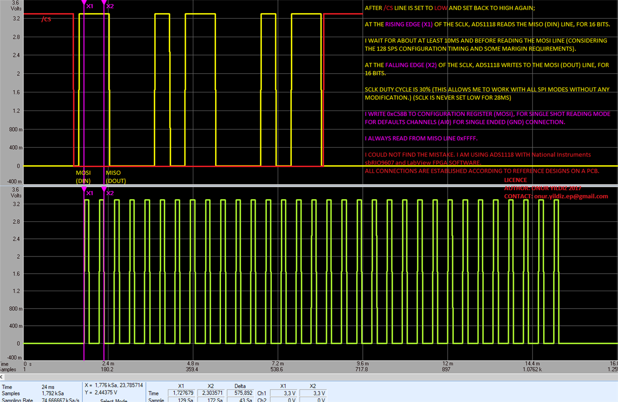
In my circuit, I could not read any value except 0xFFFF. My voltage supply is 3.3V. FSR 2.048V is choosen. 128SPS is used. Internal temperature mesaurement is also tried but MISO line is still 0xFFFF. Input and Output waveforms are continuously checked by an oscilloscope. Upper waveform is prepared for just a simple illustration and clarifying the issue. Top waveform is MOSI, and Bottom waveform is SCLK. In-Pic information is also provided in below:

Best Regards,

ONUR YILDIZ

"AFTER /CS LINE IS SET TO LOW AND SET BACK TO HIGH AGAIN;AT THE RISING EDGE (X1) OF THE SCLK, ADS1118 READS THE MISO (DIN) LINE, FOR 16 BITS.

I WAIT FOR ABOUT AT LEAST 10MS AND BEFORE READING THE MOSI LINE (CONSIDERING THE 128 SPS CONFIGURATION TIMING AND SOME MARIGIN REQUIREMENTS).

AT THE FALLING EDGE (X2) OF THE SCLK, ADS1118 WRITES TO THE MOSI (DOUT) LINE, FOR 16 BITS.

SCLK DUTY CYCLE IS 30% (THIS ALLOWS ME TO WORK WITH ALL SPI MODES WITHOUT ANY MODIFICATION.) (SCLK IS NEVER SET LOW FOR 28MS)

I WRITE 0xC58B TO CONFIGURATION REGISTER (MOSI), FOR SINGLE SHOT READING MODE FOR DEFAULTS CHANNELS (AI0) FOR SINGLE ENDED (GND) CONNECTION.

I ALWAYS READ FROM MISO LINE 0xFFFF.

I COULD NOT FIND THE MISTAKE. I AM USING ADS1118 WITH National Instruments sbRIO9607 and LabView FPGA SOFTWARE.

ALL CONNECTIONS ARE ESTABLISHED ACCORDING TO REFERENCE DESIGNS ON A PCB."

  • Hi Onur,

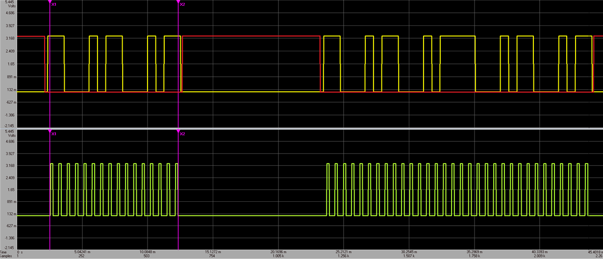
    Welcome to the forum! The ADS1118 will communicate in full-duplex which means that the device will transmit data in the same clock sequence as it is received from the master.  Unfortunately only the transmit data is shown in your scope shot.  I also see that the you are issuing a 32 clocks to the ADS1118 but bring CS high after the first 16 clocks are issued.  It would be helpful to see the data response from the ADS1118 to verify your configuration was properly written. Is it possible to hold CS low for all 32 clocks and show a scope shot of CS, SCLK, DIN and DOUT all at the same time?

    You have stated that your result is 0xFFFF which is actually one code below 0V input in binary 2's complement.  What input voltage do you have connected to AIN0?  And what result do you expect to see?

    Best regards,

    Bob B

  • Hi Bob,

    For just in order to test the response of ADS1118,  internal temperature measurement, I expect like one of this possible hex codes, according to stepsize of the sensor, ex. 0x0640. But it is 0xFFFF all the time.

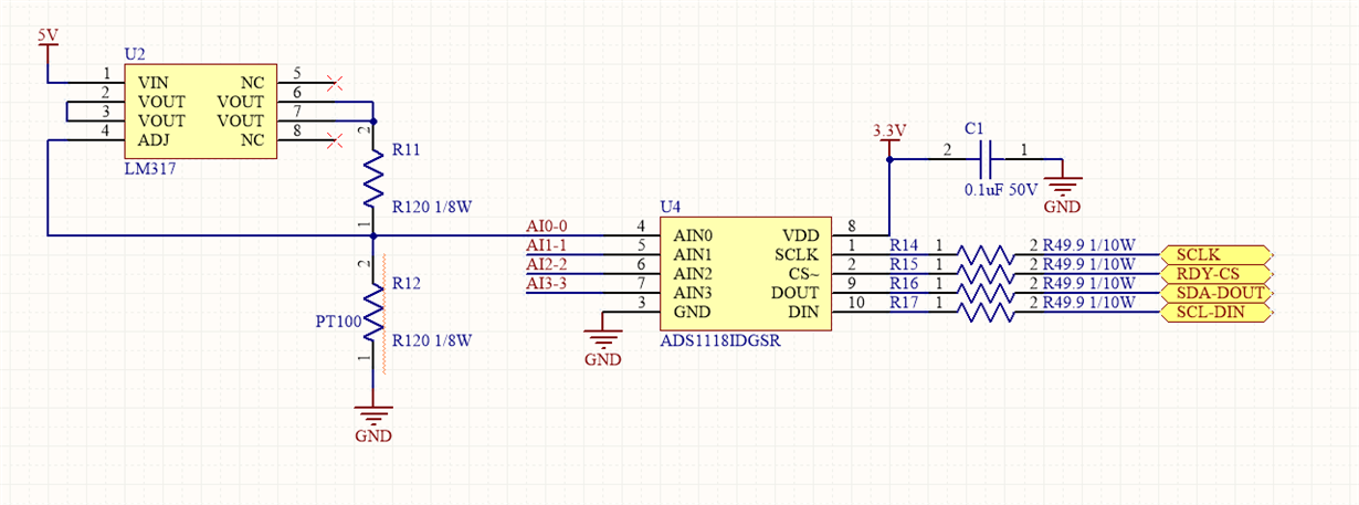
    For ADC, I am using a PT100 temperature sensor connected to a current source, LM317. It is in a isolated test lab, and unfortunately it is also forbidden to take any photo. Because of that I can not take the actual photo of oscilloscope screen or any other, But my expected value is about ~1.25V with an error of max 12mV (20 degree C Temperature). I also test it with precise resistances, i.e. 120 Ohms with %0.1 error, and I expect 1.25V measurement typical. Oscilloscope and Digital Multimeter (since it is considered as a slow moving signal) shows a clear potential of 1.24V for ADC Input line 0 of ADS1118. My simplified circuit connection is below:

    I tried to change the voltage level on AIN0 but ADC measurement is still 0xFFFF. I see only a straight HIGH level on MISO. My expected value for 1.25V Input is 0x4E20 (binary 0100 1110 0010 0000 and it is the 20000th step of total 32768steps) for FSR 2.048V since I use single ended connection (I lose 1 MSBit and my stepsize for ADC is 62.5uV, which gives me total of 32768 steps).

    Changing SCLK for 16 bit or 32 bit makes no differance, I also set /CS according to 16bit or 32bit orderly, but no change in the MISO (DOUT).

    What do you think about this waveforms, what might be the problem, should not it work properly? There might be a hardware fail for ADS1118, I will check for it if my timing, configuration and connections are properly designed. MOSI line is 0xC58B. Any other value other than 0xFFFF is welcome for me, which would show me a real response from the ADS1118.

  • Hi Onur,

    Unfortunately you did not send me what I asked for, you only sent CS, SCLK and MOSI (DIN).  I do not see the DOUT, so I cannot verify if the device is communicating at all.  If DOUT is always high even for the second half of the 32 SCLKs issued, then I would think that you have a connection problem with one of the digital signal lines to the ADS1118.  Perhaps a poor solder connection for the series resistors or perhaps at the ADS1118 itself.  I would suggest probing directly on the pins of the ADS1118 to verify proper communication. Based on the information I have so far I would say that the configuration is not getting to the ADS1118.

    Best regards,

    Bob B

  • Hi Bob,

    Thank you very much and I am really appreciated to you for your solution suggestions about the problem. I was on my vocation and I could not reply to you. I have solved the problem. It was sourcing from the written digital signal, it was sent to the MOSI line unfortunately in the reverse order.

    Best Regards,

    Onur YILDIZ