This thread has been locked.

If you have a related question, please click the "Ask a related question" button in the top right corner. The newly created question will be automatically linked to this question.

ADS1294: ocular EMG signal

Part Number: ADS1294

Hi, my name is Juan from Argentina. 

I would like to use ADS1294 to make a project which constist on sensing eye blinking but I have some questions:

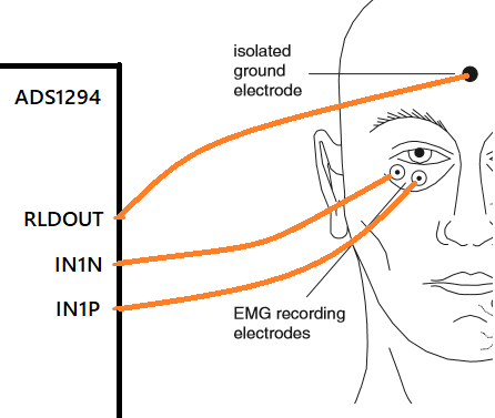
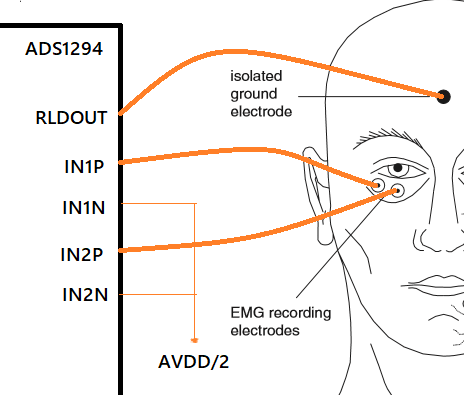
1) As regard to connection, I have two options:

a-

b- 

I am considering to use an unipolar supply (0V - 5V), so I dont know if the two options are correct and which one is the best with this supply method. Could you help me?

2) In two pictures, I connect RLD electrode to RLDOUT but I read that it can connect to RLDIN and then this signal can be rerouting to any of channel input. What are the differences? Any advantage?

3) As regard to isolate the device from the human body, an optoisolator is recommend. Are they necessary in all inputs or only at RLDOUT? Do you have any CI to recommend in TI?

4) Before channel input, I am thinking to use a band pass filter (Low pass filter: 500Hz and High pass filter:28Hz). Is first order filter enough?

Thank you.


  • Hello Juan,

    Thanks for your interest in the ADS1294!

    While we're not the application experts, I can try to guide you with the following recommendations below:

    1. The answer to your first question really depends on whether you need the unique information that is sensed by each electrode input. If you only care about the differential voltage, then you could reduce the number of required channels and potentially design a cheaper solution. The single-ended approach (technically "pseudo-differential") with INxN tied to mid-supply will also work. Ideally, RLDOUT will be centered around the same mid-supply, so the differential voltage will be centered around 0V while allowing you to still use the ADC's full-scale range. You could always measure each electrode independently with two channels, then subtract the results in post-processing if you also care about the differential voltage.
    2. RLDIN can be used to route the RLDOUT signal into the input MUX and out to one of the channel input pins. At that time, the input pin becomes disconnected from the internal PGA. This is useful when the RLD electrode is disconnected. A simple register change can reroute the biasing signal to the body temporarily until the RLD electrode connection is restored. Also, RLDIN can be used to directly measure RLDOUT against mid-supply to check the common-mode signal that is driven to the body. This would disconnect the PGA from the INxx pins once again and use the MUX to route RLDOUT to the selected channel.
    3. I'm not sure about this one. We really don't have much experience when it comes to isolation techniques used in medical systems. I don't believe this technique is absolutely necessary, however, as long as you have sufficient protection circuitry in place. This would include current-limiting resistors and clamping diodes to protect the patient and the measurement circuitry from over-voltage and momentary increases in DC current.
    4. The filter is really up to your application requirements. I think many customers can remove the DC content in the digital domain with a higher-order high-pass filter, which is easier to implement than in the analog domain. The analog low-pass filter could be increased to a second order - many times multiple R-C pairs are used to increase protection while providing extra filtering at the same time. The signal bandwidth, again, is up to you, but the important detail for your filter design is that it should provide sufficient antialiasing by the ADC modulator frequency (fMOD). This is where the digital filter respond returns to unity-gain (0 dB) and noise can alias back into your signal bandwidth. See Figures 52-56, where fMOD is either fCLK / 4 or fCLK / 8, depending on the mode. A second-order low-pass filter at 500Hz would give you -120dB attenuation at 500kHz, which I think is more than enough. You could extend the cutoff further to 5kHz so as not to interfere with your signal bandwidth, or use a simple single-order filter.

    I hope that helps!

    Best Regards,

  • Hi Ryan Andrews,

    Thank you for your answer.

    I want to check your comments because I didnt understand two phrases:

    Answer 1)  "Ideally, RLDOUT will be centered around the same mid-supply, so the differential voltage will be centered around 0V "

    Questions:

    Differential voltage between?

    I have understood that RLD is a negative feedback but how this affect the body? Why RLD signal is the mid-supply?

    If you could explain RLD function better, I will appreciate it.

    Answer 2) "This is useful when the RLD electrode is disconnected. A simple register change can reroute the biasing signal to the body temporarily until the RLD electrode connection is restored"

    Question:

    Which is the biasing signal?

    I understood the other part of the answer but I have a problem with this phrase so I cant see the advantage of using RLDIN and MUX in place of using RLDOUT directly.

    Thank you again.

    Juan

  • Hello Juan,

    RLD stands for Right-Leg Drive. This is special electrode signal that serves two purposes in ECG and other biopotential applications:

    1. First, it sets the patient's DC common-mode voltage so that the signals measured from the body are within range of the measurement subsystem. Otherwise, the body is basically floating and the DC common-mode voltage is undefined.
    2. Second, the RLD signal is typically generated to carry an AC common-mode cancellation signal. This greatly helps to improve system common-mode rejection (CMR), which is a strict IEC standard for medical equipment. This becomes particularly important for rejecting 50Hz/60Hz power line noise.

    For more information about RLD and improving CMR, check out our online ECG training series as well as an application note dedicated to this very topic:

    The output of the RLD amplifier is centered around the DC common-mode voltage that is connected to the amplifier's non-inverting input. The ADS1294 can set this voltage to mid-supply through an internal resistor divider. More information about configuring the RLD amplifier can be found in section 9.3.1.7.6.

    Rerouting or measuring the RLDOUT signal is explained in sections 9.3.1.7.1 and 9.3.1.7.2, respectively. I did not mean to suggest that RLDIN offered an advantage over RLDOUT directly - instead, it can be used as a "fallback" plan just in case the RLD electrode is disconnected. You don't want the body to float relative to the measurement system.

    Best Regards,

  • Hello Ryan,

    Thank you again for your time and your explanations, I am solving my problems.

    However, I cant understand about rerouting signal. I understand how it works, which registers I need to configure, etc., but I cant see why you say that the body doesnt float relative to measurement system without RLD electrode connected. Why? How can I keep common-mode voltage without RLD electrode?

    How can I reroute biasing signal without this?

    On the other hand, I continue not understanding what biasing signal is. Sorry for my ignorance.

    Thank.

    Juan

  • Hello Juan,

    Asking questions is perfectly fine. Did you go through the presentation training? There is a section dedicated to what RLD is and why it's needed.

    In my previous response, I said that the body does float without RLD. The DC common-mode voltage of the body is undefined. If you do not wish to use the RLD, you can AC-couple the electrode inputs instead and bias the signals with a resistor divider, for example. In that scenario, the DC voltage of the body does not matter since the series AC-coupling capacitors will block DC signals.

    I suggest not worrying about rerouting the RLD output for now. Again, this feature is merely a backup plan for systems which bias the body through RLD.

    Best Regards,

  • Hello Ryan,

    I have been designing a board to test EMG signal and I have a doubt about protection circuit. I have read "Improving commom-mode rejection using the Right Leg Drive Amplifier" application note and I dont know how to select Cp value.

    In the paper says: "The value of CP is chosen such that zero as a result of RP and CP is approximately 60 Hz". In my case I have a RP = 120k and I would like to have that zero at 50Hz. How could I find the value of Cp? What is the equation?

    Thanks,

    Juan 

  • Hello Juan,

    I have a feeling that this is a typo in the application note.

    The concept behind this Rp || Cp combination is that you are introducing a zero in the feedback loop of the RLD amplifier that will offset the pole created by the cable resistance and parasitic capacitance. This pole will be much greater than 50 Hz or 60 Hz - likely a few 10s of kHz or even 100s of kHz. To set Rp and Cp appropriately, try to find any information about the series impedance or parasitic capacitance of the ECG cables in your system.

    For an example, you can assume something like 100pF (Ccb). If the nominal cable impedance is 10k (Rcb), that would put the pole around 159kHz.

    The zero from Rp || Cp should be set to cancel this pole from the cables. With Rp = 120k, the Cp value you need would be (1/(2*pi*159k*120k) ~= 8.3pF.

    Best Regards,
  • Hello Ryan,

    First of all, thanks for your last answer.

    In this case, I was trying to do first tests when a new problem appear. DOUT pin was connected to an Arduino Nano which was connected to a PC with the idea to see a signal wave (I was using internal test signal) but the output value was noise.

    Then I measured the voltage on VREFP pin and it was zero (100mV). So, here is my doubt, I have two possible causes:

    1) Schematic problem (connection problem) because if the ads was switched on, the default value at this pin should be 2.4V.

    2) The ADS is off due to a problem in SPI communication.

    I dont know if this is a common problem and you have a solution or if I can send you schematic and initial routine.

    If you have an arduino or LPC1769 code in which figure configuration and initial routine, could help me.

    Thanks

    Juan
  • Hi Juan,

    Are you trying to use the internal reference voltage? It sounds like the internal reference buffer is powered-down, which is the default setting. To enable it, set CONFIG3[7] to '1.' As you mentioned, you should measure 2.4 V between VREFP and VREFN.

    Let me know if that works.

    Best Regards,
  • Yes, I am using internal reference voltage and that bit is configured like you said. So, I believe that the problem is SPI communication. However, I am using a tested SPI Arduino Library that's why I think the problem is in initialitation routine.

    This is:

    void init_ADS1294( void )
    {
    /*power up secuence*/
    digitalWrite(PIN_PWDN,HIGH);
    digitalWrite(PIN_RESET,HIGH);

    delay(tPORT*MS);

    digitalWrite(PIN_RESET,LOW);
    delay(tCLOCK*2*MS);
    digitalWrite(PIN_RESET,HIGH);

    delay(16*tCLOCK);

    Serial.println("init_ADS");
    /*Configuración de registros*/
    wReg(CONFIG3_ADDRESS,CONFIG3);
    wReg(CONFIG1_ADDRESS,CONFIG1_LP_1K);
    wReg(CONFIG2_ADDRESS,CONFIG2);
    wReg(LOFF_ADDRESS,LOFF);
    wReg(CH1SET_ADDRESS,CHxSET_TEST);
    wReg(CH2SET_ADDRESS,CHxSET_OFF);
    wReg(CH3SET_ADDRESS,CHxSET_OFF);
    wReg(CH4SET_ADDRESS,CHxSET_OFF);
    wReg(RLD_SENSP_ADDRESS,RLD_SENSP);
    wReg(RLD_SENSN_ADDRESS,RLD_SENSN);
    wReg(LOFF_SENSN_ADDRESS,LOFF_SENSN);
    wReg(LOFF_SENSN_ADDRESS,LOFF_SENSP);
    wReg(LOFF_FLIP_ADDRESS,LOFF_FLIP);
    wReg(CONFIG4_ADDRESS,CONFIG4);

    /*Start convertion*/
    enviarDatoSPI(RDATAC);
    enviarDatoSPI(START);
    enviarDatoSPI(SDATAC);
    }
  • Hello Juan,

    SDATAC must be sent before any other commands, otherwise they will not be recognized. After configuring the registers, you should read them all back to confirm they were written correctly.

    Once you are done configuring the device and you've confirmed the settings, then you can send RDATAC again.

    Best Regards,
  • Hello Ryan,

    I was sending SDATAC before any other command, but it was in another function.

    After configuring registers, I added code to read them. It saves the data in a variable (initial value = 0) but when I print this, the value is zero. I believe that SPI.transfer isnt working or ADS has problem.

    I have some question:

    1) How can I know if ADS was started properly? Can I measure some pin?

    2) What is SCLK max rate? 20MHz? I am using DVDD = 3.3V and DGND = 0V.

    3) What is the max current input that the device consumes?

    4) How can I verify if the device isnt burned?

    5) Should AGND and DGND be connected? Both of them are 0V.

    6) Do you have an schematic example to see or can I send you mine?

    7) Do you have an Arduino or LPC code example to see?

    I have less than 2 months to present the project and I cant start. I hope you can help me.

    Really thanks.

    Juan

  • Hello Ryan,

    As regard to my last answer, I can solve some problems and I read back registers with RREG. However, the device isnt working well.

    1) I measured clk pin (I am using internal clock oscillator) and I could see a frecuency signal of 2Mhz but isnt rectangular,  it had a lot of distortion. It depend on osciloscope bandwidth?

    2) If I make a new code in which I only do start up secuency and tie start pin to HIGH, what should be frecuency signal in DRDY pin?

    Thanks you again.

    Juan

  • Hello Juan,

    If START is tied high to DVDD during start-up, then /DRDY will begin pulsing at the default data rate (500SPS).

    One trick to probing clock signals is to use the shorted ground wire possible for your probe. Also, try probing the clock as close as possible to the CLK pin and connect the ground wire to the nearest point.

    Best Regards,
  • Hello Ryan,

    Thanks for your last answer.

    I am seeing a little progress in my project. In this occasion, I have a punctual doubt.

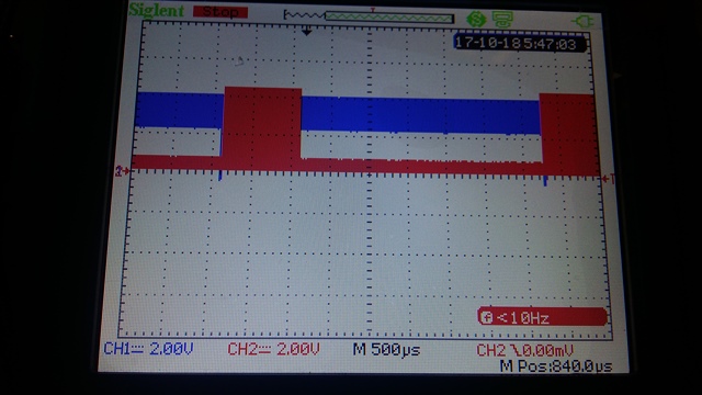
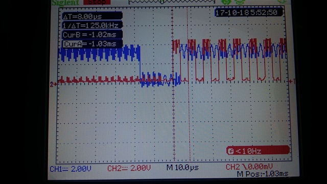
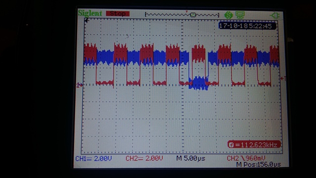
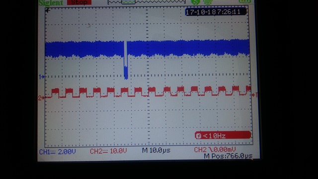
    First, I started the device with default settings and I could see:

    CH1 - BLUE - DRDY

    CH2 - ORANGE - SCLK

    I measured time between two DRDY pulse and this agree with 250sps. In addition, I could count 120 SCLK pulses (24 status bits and 4x24 channel bits). Have signals a lot of noise?

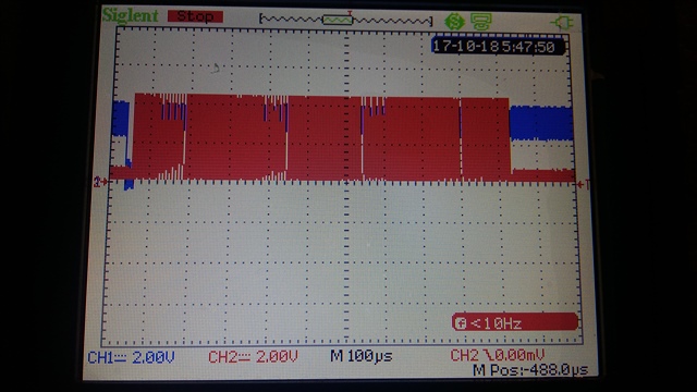
    Then, I tried changing the mode to HP and the result doesnt match with datasheet. DRDY signal changed according to the new data rate (500sps) but SCLK have the problem showed in the following images, it isnt synchronized with DRDY falling edge and there are more than 120 pulses. So, I came back to the beginning with default settings but  the problem with SCLK still there, (The images below are with default settings)

    I hope you can help me. Thank you again.

    Juan