This thread has been locked.

If you have a related question, please click the "Ask a related question" button in the top right corner. The newly created question will be automatically linked to this question.

ADS1262: Problem when trying to read more than 60sps

Part Number: ADS1262

Hello, i'm using ADS1262 to read data from a Load Cell using an Arduino UNO.

I'm using a board designed from protocentral: "PROTOCENTRAL ADS1262 32-BIT PRECISION ADC BREAKOUT BOARD"

When I configure to read until 60sps it works perfecly.

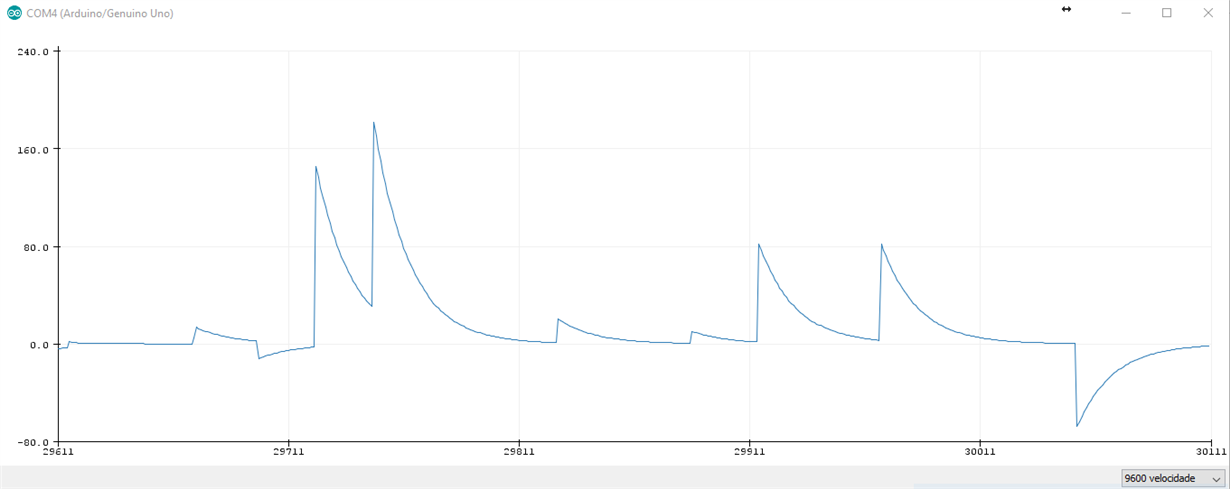
But when I try to get more samples, 100+ it starts to appear lots of spikes in the data.

I saw that i cannot use FIR filter to more than 20sps. 
I tryed using sinc1 to sinc4 but neither works.

What am I doing wrong?

Thank you.

  • Some info:

    ads1262_Reg_Write(POWER, 0x11);
    ads1262_Reg_Write(INTERFACE, 0x05);
    ads1262_Reg_Write(MODE0, 0x00); //continuous conversion on, chopp and IDAC rotation off, no delay
    ads1262_Reg_Write(MODE1, 0x60); //sync4
    ads1262_Reg_Write(MODE2, 0x36); //8V/V, 60sps... Here when I change to more than 60sps the error begin
    ads1262_Reg_Write(INPMUX, 0x01);
    ads1262_Reg_Write(OFCAL0, 0x00);
    ads1262_Reg_Write(OFCAL1, 0x00);
    ads1262_Reg_Write(OFCAL2, 0x00);
    ads1262_Reg_Write(FSCAL0, 0x00);
    ads1262_Reg_Write(FSCAL1, 0x00);
    ads1262_Reg_Write(FSCAL2, 0x40);
    ads1262_Reg_Write(IDACMUX, 0xBB);
    ads1262_Reg_Write(IDACMAG, 0x00);
    ads1262_Reg_Write(REFMUX, 0x00);
    ads1262_Reg_Write(TDACP, 0x00);
    ads1262_Reg_Write(TDACN, 0x00);
    ads1262_Reg_Write(GPIOCON, 0x00);
    ads1262_Reg_Write(GPIODIR, 0x00);
    ads1262_Reg_Write(GPIODAT, 0x00);
    ads1262_Reg_Write(ADC2CFG, 0x00);
    ads1262_Reg_Write(ADC2MUX, 0x01);
    ads1262_Reg_Write(ADC2OFC0, 0x00);
    ads1262_Reg_Write(ADC2OFC1, 0x00);
    ads1262_Reg_Write(ADC2FSC0, 0x00);
    ads1262_Reg_Write(ADC2FSC1, 0x40);
  • Hi Eduardo,

    Welcome to the TI E2E Forums!

    Have you tried probing your SPI signals while reading data?

    Since you are only see issues reading data at the higher data rates then I would look to see if you are reading the data in time (before the next ADC conversion is completing). If you clock out the data without the RDATA1 command, you are at risk of corrupting the data should you be reading data while the conversion completes. The RDATA1 command will save the old conversion data to a buffered output shift register so that new data does not overwrite your old data.

    Also it would help to know what SCLK frequency you're using and whether or not you're polling the /DRDY pin or using a /DRDY interrupt to determine when to read data?

    Thanks,
    Chris
  • Hello Christopher,

    Sorry for the time I took to answer your reply, I had to study very deep ADS1262 datasheet before replaying.

    Well, when I created the post I was doing lots os wrong things, including not calling RDATA1 command.
    I've made some good changes and I'm able to get until 7200sps.

    SCLK frequency is configured on 2000000Hz (SPI_CLOCK_DIV8).
    I'm monitoring /DRDY pin to see when data is ready to read but during this time I'm not doing any data transfer. Is this wrong?

    The problem is that I'm not sure if since I'm using a generic code I created to count and I'm not verifying if the data is new, still don't know how to do.
    Besides, when I set to 14400 sps, it counts about 12000 sps, and when I try to get more it takes maximum of 15000sps.

    Is there others configurations I need to look or change?
    My code (arduino) is written below.

    Thank you Chirs. 

    Eduardo.

    /*Wiring to your Arduino
     example.ino
     this example gives differential voltage across the AN0 And AN1 in mV
     Hooking-up with the Arduino
    ----------------------
    |ads1262 pin label| Pin Function         |Arduino Connection|
    |-----------------|:--------------------:|-----------------:|
    | DRDY            | Data ready Output pin|  D6              |             
    | MISO            | Slave Out            |  D12             |
    | MOSI            | Slave In             |  D11             |
    | SCLK            | Serial Clock         |  D13             |
    | CS              | Chip Select          |  D7              |
    | START           | Start Conversion     |  D5              | 
    | PWDN            | Power Down/Reset     |  D4              |
    | DVDD            | Digital VDD          |  +5V             |
    | DGND            | Digital Gnd          |  Gnd             |
    | AN0-AN9         | Analog Input         |  Analog Input    |
    | AINCOM          | Analog input common  |                  |
    | AVDD            | Analog VDD           |  -               |
    | AGND            | Analog Gnd           |  -               |
    -----------------------------------------------------------------
    */
    #include <SPI.h>
    #include <SoftwareSerial.h>
    #include <math.h>
    
    #define PGA 1 // Programmable Gain = 1
    #define VREF 2.50 // Internal reference of 2.048V
    #define VFSR VREF/PGA //2.50/1 = 2.50             
    #define FSR (((long int)1<<23)-1)  
    
    int CONFIG_SPI_MASTER_DUMMY = 0xFF;
    // Register Read Commands
    #define RREG 0x20
    #define WREG 0x40
    #define START 0x08
    #define STOP 0x0A
    #define RDATA 0x12
    
    //Pins used for the connection with the sensor, the other you need are controlled by the SPI library):
    const int ADS1262_DRDY_PIN = 6;
    const int ADS1262_CS_PIN = 7;
    const int ADS1262_START_PIN = 5;
    const int ADS1262_PWDN_PIN = 4;
    //Register address
    #define POWER 0x01 //11h (default)
    #define INTERFACE 0x02 //05h (default)
    #define MODE0 0x03 //00h (default)
    #define MODE1 0x04 //80h (default)
    #define MODE2 0x05 //04h (default)
    #define INPMUX 0x06 //01h (default)
    #define OFCAL0 0x07 //00h (default)
    #define OFCAL1 0x08 //00h (default)
    #define OFCAL2 0x09 //00h (default)
    #define FSCAL0 0x0A //00h (default)
    #define FSCAL1 0x0B //00h (default)
    #define FSCAL2 0x0C //40h (default)
    #define IDACMUX 0x0D //BBh (default)
    #define IDACMAG 0x0E //00h (default)
    #define REFMUX 0x0F //00h (default)
    #define TDACP 0x10 //00h (default)
    #define TDACN 0x11 //00h (default)
    #define GPIOCON 0x12 //00h (default)
    #define GPIODIR 0x13 //00h (default)
    #define GPIODAT 0x14 //00h (default)
    #define ADC2CFG 0x15 //00h (default)
    #define ADC2MUX 0x16 //01h (default)
    #define ADC2OFC0 0x17 //00h (default)
    #define ADC2OFC1 0x18 //00h (default)
    #define ADC2FSC0 0x19 //00h (default)
    #define ADC2FSC1 0x1A //40h (default)
    
    float volt_V=0;
    float volt_mV=0;
    volatile int i, data;
    volatile char SPI_RX_Buff[10];
    volatile long ads1262_rx_Data[10];
    volatile static int SPI_RX_Buff_Count = 0;
    volatile char *SPI_RX_Buff_Ptr;
    volatile int Responsebyte = false;
    volatile signed long sads1262Count = 0;
    volatile signed long uads1262Count=0;
    double resolution;
    
    unsigned long inicio=0;
    int contador1, contador2=0;
    int celula = 1;
    
    void setup() 
    {
      // initalize the  data ready and chip select pins:
      pinMode(ADS1262_DRDY_PIN, INPUT); //Data ready input line
      pinMode(ADS1262_CS_PIN, OUTPUT); //Chip enable output line
      pinMode(ADS1262_START_PIN, OUTPUT); //Start 
      pinMode(ADS1262_PWDN_PIN, OUTPUT); //Power down output
    
      digitalWrite(ADS1262_START_PIN, LOW); //Manter o pino LOW e controlar comunicação via código SPI
      digitalWrite(ADS1262_CS_PIN, LOW); //Manter o pino LOW para manter comunicação sempre possível
    
      Serial.begin(115200); //inicia comunicação serial
      SPI.begin(); // start the SPI library:
      SPI.beginTransaction(SPISettings(20000000, MSBFIRST, SPI_MODE1));
      ads1262_Init(); // initialise ads1262 slave
      
      inicio = millis();
     }
    
    void loop() 
    {
      while (digitalRead(ADS1262_DRDY_PIN) == HIGH){ //while data is not ready - do nothing
        //Serial.print(","); 
      }
      
      //LER OS DADOS
      SPI_RX_Buff_Ptr = ads1262_Read_Data();  //6Bytes <STATUS|DATA1|DATA2|DATA3|DATA4|CHECKSUM>
    
      for(i = 0; i <5; i++) //Remove STATUS byte?
      {
        SPI_RX_Buff[SPI_RX_Buff_Count++] = *(SPI_RX_Buff_Ptr + i);              
      }
      
      if(SPI_RX_Buff_Count >= 5)  {
        ads1262_rx_Data[0]= (unsigned char)SPI_RX_Buff[1];  // read 4 bytes adc count
        ads1262_rx_Data[1]= (unsigned char)SPI_RX_Buff[2];
        ads1262_rx_Data[2]= (unsigned char)SPI_RX_Buff[3];
        ads1262_rx_Data[3]= (unsigned char)SPI_RX_Buff[4];
        
        uads1262Count = (signed long) (((unsigned long)ads1262_rx_Data[0]<<24)|((unsigned long)ads1262_rx_Data[1]<<16)|(ads1262_rx_Data[2]<<8)|ads1262_rx_Data[3]);//get the raw 32-bit adc count out by shifting
        sads1262Count = (signed long) (uads1262Count);      // get signed value
        resolution = (double)((double)VREF/pow(2,31));       //resolution= Vref/(2^n-1) , Vref=2.5, n=no of bits
        volt_V      = (resolution)*(float)sads1262Count;     // voltage = resolution * adc count
        volt_mV   =   volt_V*1000;                           // voltage in mV
        Serial.println(volt_mV);
        //Serial.println(" mV");
        }
        SPI_RX_Buff_Count = 0;
        
    //VERIFYING THE NUMBER OF SAMPLE RATE OUTPUT contador1++; if (millis() - inicio > 1000) { Serial.println(contador1); inicio = millis(); contador1=0; } } float mapfloat(float x, float in_min, float in_max, float out_min, float out_max) { return (x - in_min) * (out_max - out_min) / (in_max - in_min) + out_min; } void ads1262_Init() { ads1262_Reset(); delay(100); ads1262_Reg_Write(POWER, 0x11);delay(10); //11h (default) internal ref enabled ads1262_Reg_Write(INTERFACE, 0x0D);delay(10); //05h (default) Status byte enabled, Checksum enablade ads1262_Reg_Write(MODE0, 0x00);delay(10); //00h (default) Continuous Conv Mode | 0x40 Pulse conversion mode (one shot conversion) ads1262_Reg_Write(MODE1, 0x00);delay(10); //80h (default) FIR Filter | 00h sinc1 | 60h sinc4 ads1262_Reg_Write(MODE2, 0x5D);delay(10); //04h (default) PGA enabled 1V/V 20sps| 5Ch 32V/V 7200sps | 5Fh 32V/V 38400sps ads1262_Reg_Write(INPMUX, 0x01);delay(10); //01h (default) Multiplexer, AIN0 e AIN1 | 23h AIN2 e AIN3 ads1262_Reg_Write(OFCAL0, 0x00);delay(10); //00h (default) Offset Calibration Registers ads1262_Reg_Write(OFCAL1, 0x00);delay(10); //00h (default) Offset Calibration Registers ads1262_Reg_Write(OFCAL2, 0x00);delay(10); //00h (default) Offset Calibration Registers ads1262_Reg_Write(FSCAL0, 0x00);delay(10); //00h (default) Full-Scale Calibration Registers ads1262_Reg_Write(FSCAL1, 0x00);delay(10); //00h (default) Full-Scale Calibration Registers ads1262_Reg_Write(FSCAL2, 0x40);delay(10); //40h (default) Full-Scale Calibration Registers ads1262_Reg_Write(IDACMUX, 0xBB);delay(10); //BBh (default) Output Multiplexer, no connection, no connection ads1262_Reg_Write(IDACMAG, 0x00);delay(10); //00h (default) Current magnitude, off ads1262_Reg_Write(REFMUX, 0x00);delay(10); //00h (default) Reference Multiplexer, 2.5V, 2.5V ads1262_Reg_Write(TDACP, 0x00);delay(10);//00h (default) TDACP, no connection ads1262_Reg_Write(TDACN, 0x00);delay(10); //00h (default) TDACN, no connection ads1262_Reg_Write(GPIOCON, 0x00);delay(10); //00h (default) GPIO not connected ads1262_Reg_Write(GPIODIR, 0x00);delay(10); //00h (default) GPIO output ads1262_Reg_Write(GPIODAT, 0x00);delay(10); //00h (default) GPIO low ads1262_Reg_Write(ADC2CFG, 0x00);delay(10); //00h (default) ADC2 ads1262_Reg_Write(ADC2MUX, 0x01);delay(10); //01h (default) ads1262_Reg_Write(ADC2OFC0, 0x00);delay(10); //00h (default) ads1262_Reg_Write(ADC2OFC1, 0x00);delay(10); //00h (default) ads1262_Reg_Write(ADC2FSC0, 0x00);delay(10); //00h (default) ads1262_Reg_Write(ADC2FSC1, 0x40);delay(10); //40h (default) SPI.transfer(START); //Inicia a conversão via código 08h } char* ads1262_Read_Data() { SPI.transfer(RDATA); static char SPI_Dummy_Buff[6]; for (int i = 0; i < 6; ++i) { SPI_Dummy_Buff[i] = SPI.transfer(CONFIG_SPI_MASTER_DUMMY); //CONFIG_SPI_MASTER_DUMMY - FFh } return SPI_Dummy_Buff; // 6Bytes <STATUS|DATA1|DATA2|DATA3|DATA4|CHECKSUM> } void ads1262_Reset() //PWDN_PIN MUST BE HIGH FOR OPERATION { digitalWrite(ADS1262_PWDN_PIN, HIGH); delay(100); digitalWrite(ADS1262_PWDN_PIN, LOW); delay(100); digitalWrite(ADS1262_PWDN_PIN, HIGH); delay(100); } void ads1262_Reg_Write (unsigned char READ_WRITE_ADDRESS, unsigned char DATA) { // now combine the register address and the command into one byte: byte dataToSend = READ_WRITE_ADDRESS | WREG; // take the chip select low to select the device: SPI.transfer(dataToSend); //Send register location SPI.transfer(0x00); //number of register to wr SPI.transfer(DATA); //Send value to record into register delayMicroseconds(2); }

  • Hi Eduardo,

    I noticed that you are polling data ready and then performing the data processing/serial output. The serial output operation is likely taking a long time and preventing you from capturing data at the faster data rates. You can try disabling the serial output and using an oscilloscope to see if you're able to reading data at the full throughput; however, when outputting this data over a serial interface you might not be able to capture and display all of the data...

    I would try capturing data to memory and outputting the serial data in batches (for example, output 10 samples of data at a time). This might give you a little more data throughput.

    Best regards,
    Chris

  • Thank you Chris for the reply.

    Now I'm trying to follow topic 9.4.9.8 Calibration Command Procedure to remove offset error from my load cell. Accordingly to datasheet I must follow these steps:

    /*Calibration Command Procedure
       * 1) Enable continuous conversion (MODE 0)
       * 2) Select desired gain an reference voltage (REFMUX)
       * 3) Choose calibration type
       *    a) Offset self-calibration (automatic)
       *        Set INPMUX to FFh to open all inputs before sending calibration command
       * 4) Start conversions (send ADC1 START command)
       * 5) Send the desired calibration command (Keep CS and SCLK low during calibration)
       *    a) Offset Self-Calibration
       *        Send SFOCAL1 (19h)
       *        Set delay accordingly to Table 32
       * 6) Set INPMUX to the desired channel
    */

    I'm doing theses under "void setup()" und setting a delay of 1second after SFOCAL command except for setting SCLK low (don't know how to do it).

    It seems to do nothing, the offset is still there. 

    void arruda1262::arruda1262_Offset_Calibration (void)
    {
    	arruda1262_Reg_Write(INPMUX, 0xFF);
    	delay(10);
    	SPI.transfer(START);
    	delay(10);
    	SPI.transfer(SFOCAL1);
    	delay(1000);
    	arruda1262_Reg_Write(INPMUX, 0x01);
    }

    Is there anything wrong?

  • Hi Eduardo,

    In order to remove the external offset coming from the load cell, you'll need to perform a "system" offset calibration (SYOCAL1). The self-offset calibration only removes the ADC's internal offset, which is fairly small to begin with.

    Try programing the input multiplexer to select the load cell (with no load applied) and run the SYOCAL1 command instead. This should help remove the offset coming from the load cell.

    Best regards,
    Chris