This thread has been locked.

If you have a related question, please click the "Ask a related question" button in the top right corner. The newly created question will be automatically linked to this question.

ADS1292R: Data retrieval issue when daisy-chaining two devices

Part Number: ADS1292R

Hello TI community,

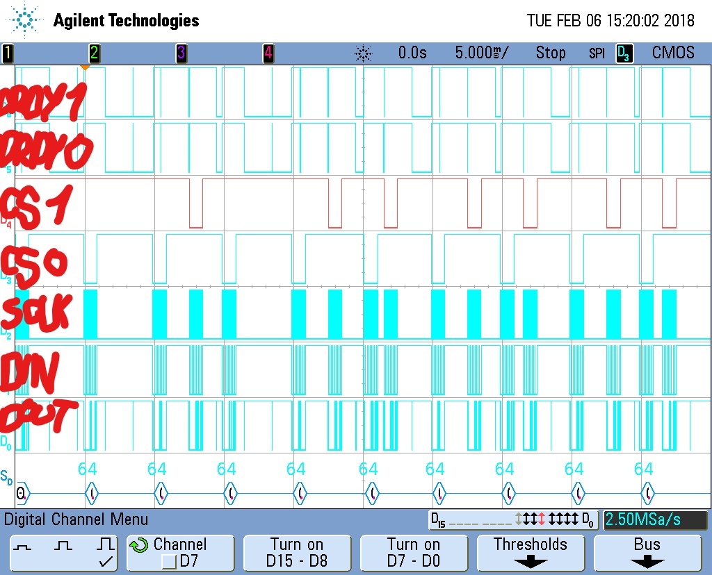
I'm currently working on the project with two ADS1292R daisy-chained, using one internal CLK as the external CLK for the other, both in RDATAC mode with test signal on the input and synchronized by toggling the START pins both with the same signal. When I start data converting, it seems that both devices DRDY signals behave the same way, even if I start communication with only one of them. This issue causes regular data collecting from one device, while the other issuing data only randomly. 

Is there anyone experienced with multiple device configuration who would be able and willing to give me any advice or have an idea what could be a problem?

Thank you very much!

  • Hello Ondrej,

    Welcome to our forum!

    Are both devices using the same clock signal? To daisy-chain multiple ADS1292R devices, each device must share the same clock signal. You can configure one device to use the internal oscillator (CLKSEL = 1) and drive the CLK pin to output the signal (CONFIG2[3] = 1). The second device can then be configured to use an external clock (CLKSEL = 0).

    If you have a schematic showing both ADS1292R devices and their surrounding input circuitry, we can take a look at that as well.

    Best Regards,
  • Hello Ryan!

    Thanks for your reply.  Yes, one ADS circuit is generating internal CLK at 512kHz, while the other circuit is taking this signal as external CLK input.

    Sure, I have the schematic, but as I said - the previous oscilloscope screenshot was taken when both circuits were configured to generate and measure internal test signal, so the input parts shouldn't have any influence on that behavior.

    I was supposing that when both circuits generate DRDY at the same time but I issue the CS signal only to one of them, the other DRDY should stay low until the program gets to the point of toggling the second CS. But both DRDY signals are doing the same no matter if the circuit is chosen by CS or not. Was my assumption correct or do I understand it wrong?

    Thanks again for your time and help.

    Sincerely

    Ondrej Strakos

  • Hi Ondrej,

    /DRDY will toggle low with each new conversion. When you are reading data, the first SCLK falling edge will clear /DRDY and force it to return high. If you do not read data, /DRDY will stay low until a few tCLK periods before the next conversion is ready.

    In your scope image, the /DRDY signals are synchronized, but you are not reading the data consistently after each /DRDY falling edge. Your MCU should treat /DRDY as an interrupt. Each /DRDY falling edge should trigger an interrupt service routine to collect the data. You need to read the data from both devices in between /DRDY falling edges. That's 2x (24 STATUS bits + 48 bits of channel data) = 144 bits. If you are reading old data when a new /DRDY falling edge occurs, the new data will overwrite the old data and begin shifting out immediately. This is is the purpose of RDATAC mode - the output shift register is updated with new conversion results automatically.

    Pay close attention to the /DRDY falling edge and allow enough time to read 144 bits before the next sample. Also, keep in mind the timing delays that are required between /DRDY and /CS as well as between /CS and SCLK.

    Best Regards,

  • Ryan,

    Thanks, really appreciate your advices. I didn't realize that since both /NDRDY signals are synchronized, I can read both device's channels at once and don't have to wait for the other device /NDRDY interrupt. This seems to give better results, even though it still skips some /NDRDY edges probably due to my program, handling some other task ...

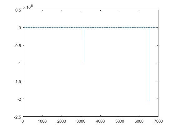
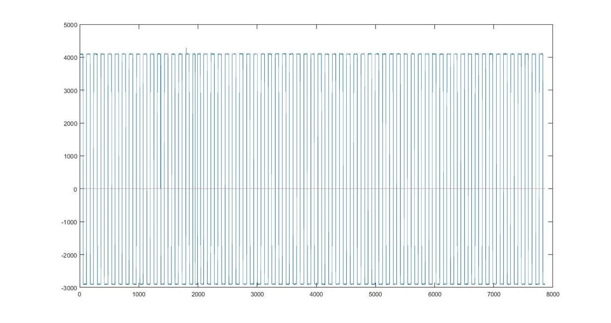
    But I'd still like to ask you two questions if you don't mind. There's some error value appearing time to time in the output stream, probably caused by some fault in data read loops and writing on memory card. But if I filter them out, the signal still sometimes looks inaccurate. Would you please be so nice and tell me if it's how is supposed to look or if there is still some problem I'm not perceiving? And what units could on the Y axis? (I'm using internal 2,42V reference, test signal and PGA gain = 1).  Sorry for these probably silly questions, I'm absolute beginner in stuff like this and so even simple things are sometimes hard to understand..

    The last question relates to the RLD configuration. I'm planning to use the external RLD electrode, but from the reference manual I can't figure out how to configure it properly. If I use only one channel on one device for now and connect the RLD lead to RLDIN/RLDREF pin,  how should I set the registers so that the RLD signal would bias the input channel I'm using for measurement? I think I'm not properly understand the RLD setting in CHxSET mux and RLD_SENS register. The options in channel mux serve if I want to use the input as RLD instead normal input and RLD_SENS bits serve for calculating a value if I'm using internal RLD loop, am I right?

    Thank you very much!

    Sincerely,

    Ondrej

  • Hello Ondrej,

    The second image looks like the correct test signal waveform and amplitude. The y-axis output is in decimal codes, where one code represents the LSB size = 291.1 nV/code (1 LSB = [2*VREF / Gain / 2^24]).  7,000 codes peak-to-peak is approximately equal to 2 mVpp, which is the correct default amplitude for the internal test signal.

    The first image looks like you are missing the next /DRDY interrupt while you are still reading old data. The data in the output shift register is immediately overwritten with new data after each /DRDY falling edge. The large negative "spikes" in the output should correspond to the moments where a portion of the old data was overwritten with new data.

    The RLD amplifier does not bias the channel inputs internally. A dedicated electrode is used to connect the RLD output to the body through some protective series resistance. The DC common-mode voltage (RLDREF) is provided at the amplifier's non-inverting input, while the AC component is derived from the selected PGA outputs and connected to the amplifier's inverting input using RLD_SENS. The R||C connection between the RLDOUT and RLDINV pins is used to close the feedback loop around the internal RLD amplifier, set the DC gain, and limit the closed-loop bandwidth. RLDIN is either used to set the DC common-mode voltage for the RLD amplifier output or to measure the RLD output internally using one of the two channels. You can leave RLDIN floating if you are using the internal RLDREF voltage and if you don't need to measure RLDOUT.

    Best Regards,

  • Dear Ryan,

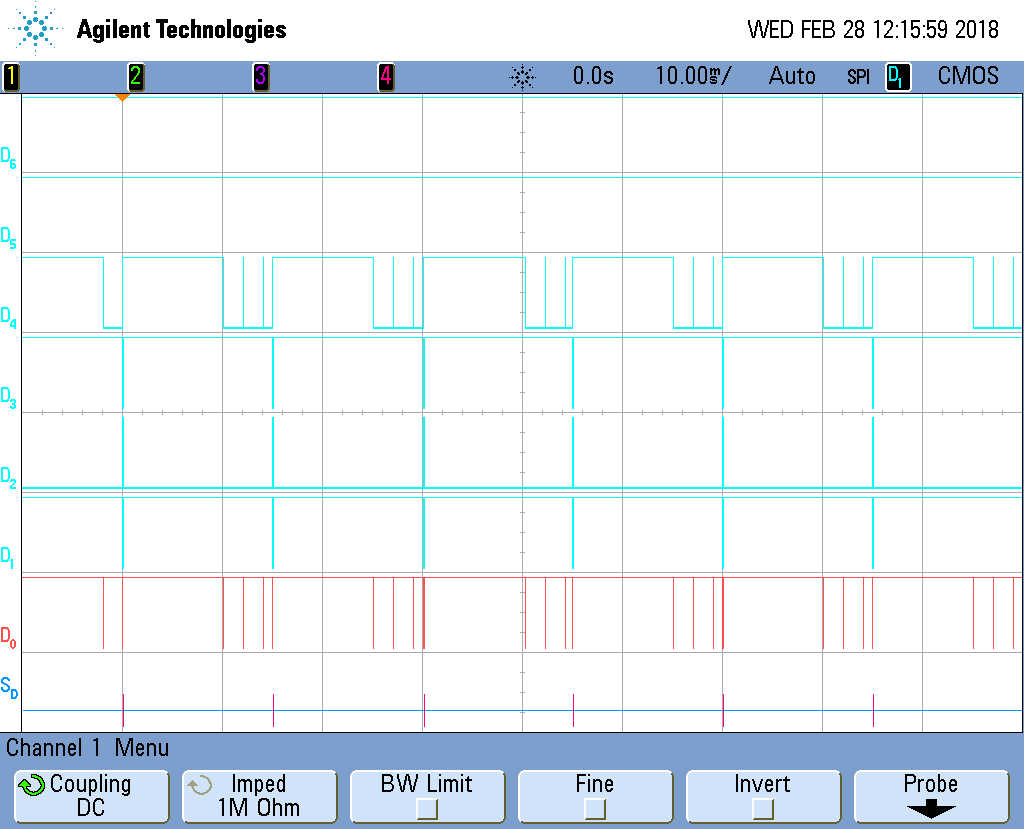
    thank you very much for your advice and explanations. I set it up according to your instructions and it was working just fine, but two days ago it suddenly started to work somehow unpredictably. When I use sampling frequency 125sps, the device usually starts giving the /NDRDY signal correspondingly first. But after few dozens of seconds (this period really varies, sometimes it's 10s, sometimes doesn't happen at all), without me changing anything, the sampling frequency either doubles, the /NDRDY interrupt signal is generated in 3edges burst (D4 line on the image) or just stays high all the time. When using any of the higher sampling frequencies, /NDRDY stays high after just cca 10s. These situations are happening randomly, no matter if I use electrode input or test signal, sometimes it happens right after power up and start and I need to turn it off and on again about 5 times to make it work again. And when any of that happens, the output values start to be either completely incorrect or just zero. 

    I've two devices on my PCB and both started to have these issues at the same time.  I probably mess something in the measuring process, but it doesn't make any sense to me, because I didn't change either the code or connection from the previous setup, where it worked without these issues. May I ask you if you have ever encountered any of these issues and have any tip how to put the devices back to normal work?

    Thank you very much!

    Sincerely,  Ondra

  • Hi Ondra,

    Are you communicating with the ADS1292R at all during this oscilloscope capture? Meaning, are you toggling the SCLK?

    The only things that can interrupt the /DRDY behavior are:

    • Setting the START pin low or sending the STOP command
    • Setting the /RESET pin low or sending the RESET command
    • Sending the STANDBY command
    • Disabling the external CLK input

    Can you probe the START, /RESET, SCLK, and /DRDY pins together without sending SCLK (i.e. hold SCLK low)? I want to verify that START and /RESET are always high and do not interrupt the /DRDY period.

    Best Regards,