This thread has been locked.

If you have a related question, please click the "Ask a related question" button in the top right corner. The newly created question will be automatically linked to this question.

ADS7871: Not able to talk with ADS7871

Part Number: ADS7871

I'm having trouble setting up this ADC through the SPI bus using an Arduino.  I tried to do some basic read commands, but I get nothing back from the chip's Dout.

Are there certain registers that need to be set up first?  I'm not using CCLK, Vref, BufIn, BufOut, or the GPIO pins.  All I have so far is setting the oscillator control to use the internal oscillator.  According to the datasheet, I need to send out 0xE0 and then 0x0C right?

If anyone has experience using this chip, any advice would be great.  Thanks,

  • Hi Andrew,

    The ADS7871 is a neat little part, but it can take a little to get it going. When you say you are not using CCLK, what do you mean? Is it open/shorted to GND/tied high? Can you provide a schematic of the area around the ADC and perhaps provide detail on your SPI control signals? The section 'Starting an A/D Conversion Cycle' (pg. 15) is a good place to start your debug process.

  • Hello Tom,

    CCLK is open which is why I need to use the internal oscillator.  I did not design the board, so I don't know the reasoning behind all the design decisions, but here is the circuitry.  

    I've read through that page in the data sheet as well as "Operating Modes", "Write Operation", and "Read Operation".  In my Arduino code, I send out 0x11 and then 0x82 to make a conversion on LN0 and read the ADC Output registers.  Does that sound correct?

  • Hi Andrew,

    Are you seeing a conversion clock output on pin 19? What voltage level do you see on the pin 26/27 side of your C9 and pin 28 side of C7?
  • On pin19, I see a clock of about 2.4MHz. Pins 26, 27, and 28 are all at 0V.

    I initially thought that I was getting nothing back from the ADC, but it seems that certain read commands do cause Dout of the chip to output. But the results don't match up with what I expect from the data sheet. For example when I try to read the ID (reg32) by sending 0xFA, I get a 0x00 instead of a 0x01, and when I try to read the A/D Control (reg3) by sending 0xC2, I get 0xFF which doesn't make sense.

  • Hi Andrew,

    OK - CCLK seems right, but it sounds like you've not got the reference enabled - take a look at the block diagram of Figure 15 (pg. 13).  By default at power up, the reference and buffer are both powered off.  Details on enabling the reference and buffer start on page 28 in the Reference/Oscillator Configuration Register section of the ADS7871 datasheet.  Can you grab a screen shot of your SPI communications and send that along?

  • Ah, I didn't know those were powered down initially.  I tried setting those bits high but still get nothing out of pins 26, 27, 28.

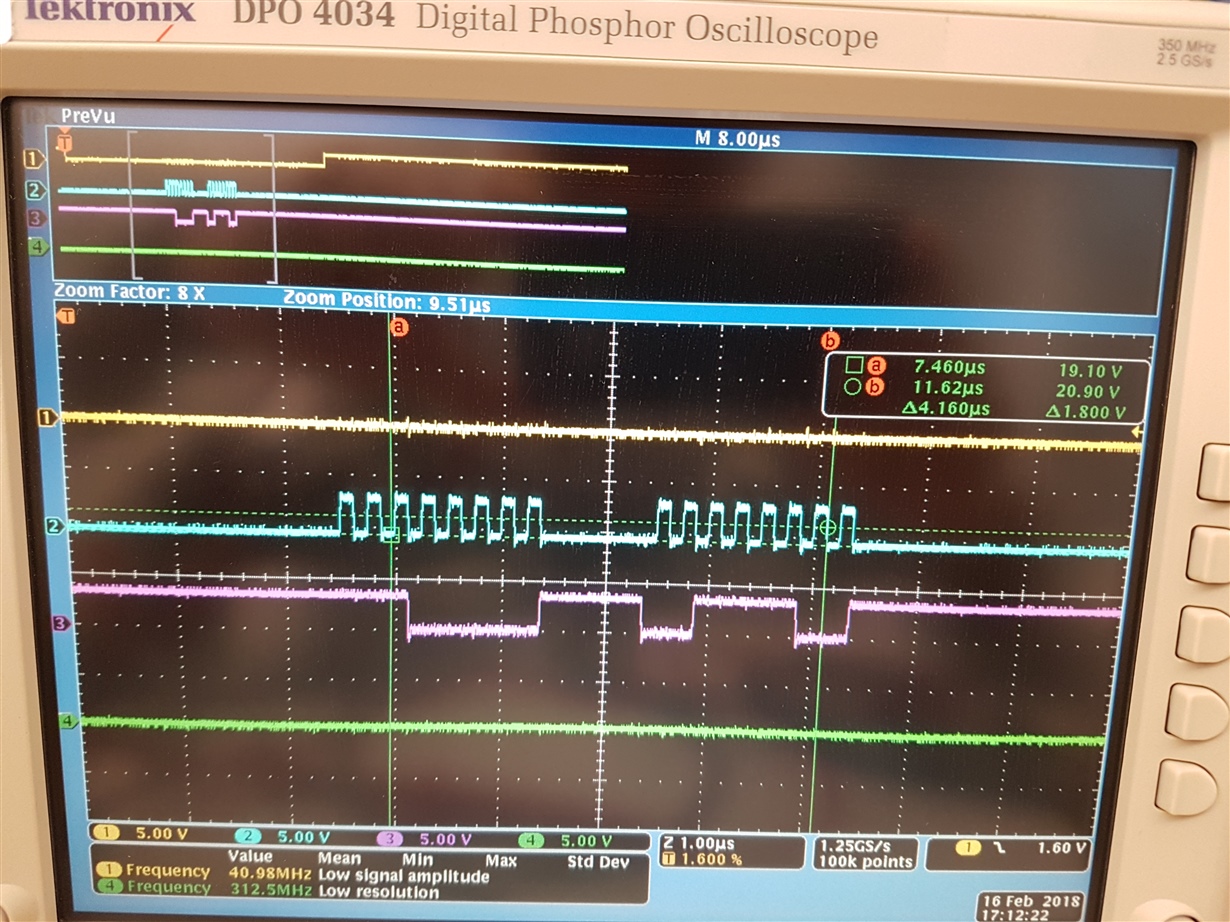
    In my code, I initially try to set the Reference/Oscillator Configuration Register by sending over 0xE0 then 0x3C:

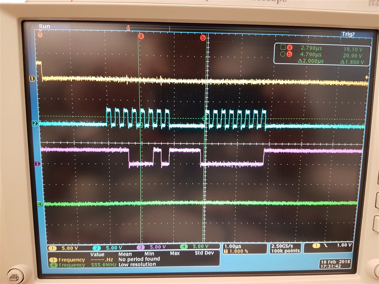
    Yellow: CS

    Blue: CLK

    Purple: Din relative to ADC

    Green: Dout relative to ADC

    Then I try to read it back by sending 0xE2 over the SPI, but get nothing back from the chip:

  • Hi Kevin,

    If you still see 0V on the ref/buffer pins, you aren't getting it enabled.  By your screen shots, you seem to be in direct mode (see Operating Modes, page 16).  To get to the reference register (ADDR7), you would need to be in register mode by starting with b00100111 (0x27) then follow with b00111100 (0x3C).  Try that and let me know if you see the reference come up.

  • Hi Tom, I'm now able to read and write to the chip.

    My original instructions weren't going through because the byte was reversed. The way the timing diagrams are drawn on your spec sheet, see pg 19 & pg 20 for the Write & Read operations, makes it seem like the byte order should be have A0 first and the mode bit last. The same applies for additional data bytes coming into the ADC or when the chip is sending data back out. I thought it was weird making us reverse the byte order and making the instructions very hard to follow. But now the way you've described it above is correct and is the more intuitive way to create the instructions.

    I was able to verify that the Ref/Osc Configuration register is b00111100, so now I get 2.5V out of BUFOUT and about 1.9V out of Vref and BUFIN.

    I do have new issue though. As I read through the 8 analog inputs, I get erratic readings. I only applied voltage to 1 of the inputs but get max readings (~16383) on some of the other inputs. It's not always the same inputs and the value can vary slightly. I checked the other inputs with a DMM and they all read 0V.

    Is this due to noise or do you think it's something else?

    -Andrew
  • Great news Andrew!  

    Yea, there are a couple LSB vs. MSB first examples, there is a bit for that in one of the registers so you can go either way.  How are you driving your inputs?  You may see some weird results with open inputs or if you have high impedance inputs directly to the ADC without a buffer in between your source and the inputs.

  • I'm driving the inputs with a digital power supply. I have 10k resistors connecting the inputs to GNDs, but those are in parallel with an open that is on my current test board. I can try it again with my newer test board that will have buffers to all the inputs lines once I get the board.
  • Hi Andrew,

    Do you have any updates for us?
  • Hello Tom, thanks for checking in.

    I don't have my other board yet. That won't be for a few weeks. I can update you then.
  • OK - No problem Andrew. I'll close this thread for now and we can get back to it once you get your boards.