This thread has been locked.

If you have a related question, please click the "Ask a related question" button in the top right corner. The newly created question will be automatically linked to this question.

ADS8548: How to write data to Configuration Register and Verify it.

Part Number: ADS8548
Other Parts Discussed in Thread: TMS570LC4357,

Hi,

I am using ADS8548 ADC with TMS570LC4357 Controller. CCS v 6.1.3.00034. I am using MIBSPIP5 to communicate to ADS8548. 

I understand from the ADS8548 Datasheet that the only conditions to write to Configuration Register is:

i) ADS8548 should be Software Mode

ii) First Bit SDI pin should be One.

Question 1: Is my above understanding correct? Or is there any additional condition to enable write to the configuration register?

If these are the only conditions, I tried writing to the configuration register with the data 0xD000_0400. I wanted to read back the data that I sent to verify if the data it was written correctly. So I sent four 16-bit data (I have verified this data on the line using scope):

1st Data: 0xD000 (CR Data)

2nd Data: 0x0400 (CR Data)

3rd Data: 0x0FFF (Dummy data to read back the CR)

4th Data: 0x0FFF (Dummy data to read back the CR)

But I did not read the data correctly. Then I checked on Pin32 Range/XCLK pin if there is any clock coming out, but there was no clock.

Question 2: Could you please help in identifying what went wrong?

Thanks in advance.

  • Hello Gobind,

    Thanks for choosing TI precision ADC.

    You are right, in order to write to the configuration register of the ADS85x8, you must set bit 31 (Write_en) followed by your desired configuration content, also SW mode is required (//HW/SW pin=high), but you will have to make sure all your pin connections for your serial interface are correct also you have to make sure your phase and polarity configuration for serial interface are correct, serial data on SDI will be latched by ADC at the falling edge of SCLK and output data are changed at the falling edge of SCLK as well.

    To verify if your serial interface and timing ae correct, please apply a DC signal on ADC's analog input, then check if your conversion code on SDO is correct without any change to Config Register, the default value in this register is 0x000003FF that means internal 2.5V reference, 4Vref range, BUSY signal etc.

    After power up ADC, just writing 0xC00003FF and then read back - you should get the 0x3FF back.

    What 's the data you got when writing and reading Config Register? if you got 0x10000400, this will be correct. Actually, 0x0400 you are writing into Config register doesn't make sense because your are using internal voltage reference by setting bit 15 to 0 but also disabling internal reference buffer by setting bit 14 to 1, I'm not sure if you want to disable internal reference instead of reference buffer.

    By the way, Range/XCLK pin is pin 34 not Pin 32, hopefully you can check pin 34.

    Please let me know your test results, thanks.

    Best regards

    Dale

  • Thanks for the reply Dale.


    I have checked:

    1. It’s in Software Mode.

    2. 31st bit is Set.

    3. Pin Connections are proper

    4. Polarity=0, Phase=1.


    I applied a DC signal of 2.5V on one of the pins without writing anything to Configuration Register, below are the results:

    In HW mode: 0x1FFF

    In SW mode: 0x06AC

    These values look incorrect to me. Please confirm.


    Then I tried writing 0xC000_03FF to config register and read it back but the results looked like they are not values from Configuration Register, but values of Channel Data. Below is the code that I used to send the data:

    Ext_ADC_ControlWord[0] = (UINT16) 0xC000;

    Ext_ADC_ControlWord[1] = (UINT16) 0x03FF;

    Ext_ADC_ControlWord[2] = (UINT16) 0x0FFF;

    Ext_ADC_ControlWord[3] = (UINT16) 0x0FFF;

    SS_SPI_WriteDataTo_TG(SPI_5, 1U, &Ext_ADC_ControlWord[0],&SS_SPI_Config_CONST);

    SS_SPI_Trigger_TG(SPI_5, 1U);


    The values that I got were:

    0x1FFF, 0xE000, 0xE000, 0xE000
    (screenshot below)


    And these values are not always the same. Sometimes I get all four values as 0xE000. Sometimes values like 0xF847, 0xF829 etc. Similar values I get when I try to read the channels. So, to me it looks like it does not matter if first bit (31st) is high or low, I get the same data.


    Another question I have is:

    If Read_EN bit of the Configuration Register is set and at the same time we have CONV_A signal. What will be the output on SDO_A? Configuration Register or Channel Data? Considering SEL_CD and SEL_B are cleared, meaning all the data goes to SDO_A in serial mode. PAR/SER pin is set to HIGH. (I am using this configuration)


    And yes, I probed on Pin 34 for the clock, not on Pin 32. Sorry for the mistake.

  • Hello Gobind,

    I will get back to you soon, thanks.

    Best regards

    Dale

  • Hi Dale,

    Just to update you, we are able to read the channel data correctly in both HW and SW mode without writing anything to Configuration Register. Meaning, if I give 2V as input to the channel, I read 2V. So, this confirms that communication connections, polarity, phase etc. are good.

    The problem is with writing to the configuration register. We are not able to write/read to/from the configuration register. Please let us know if there is anything special we should take care for writing to configuration register.

    Thank you.

  • Hello Gobind,

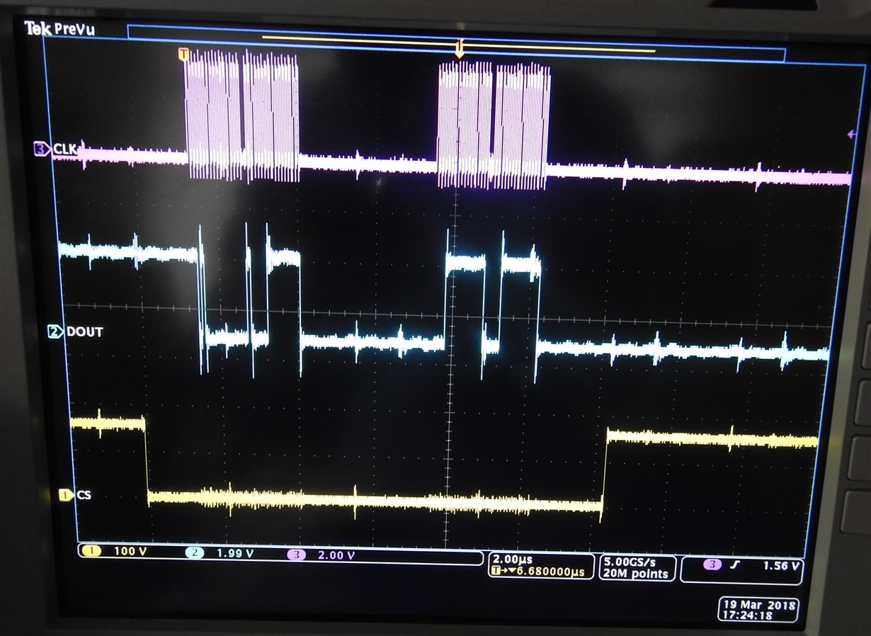
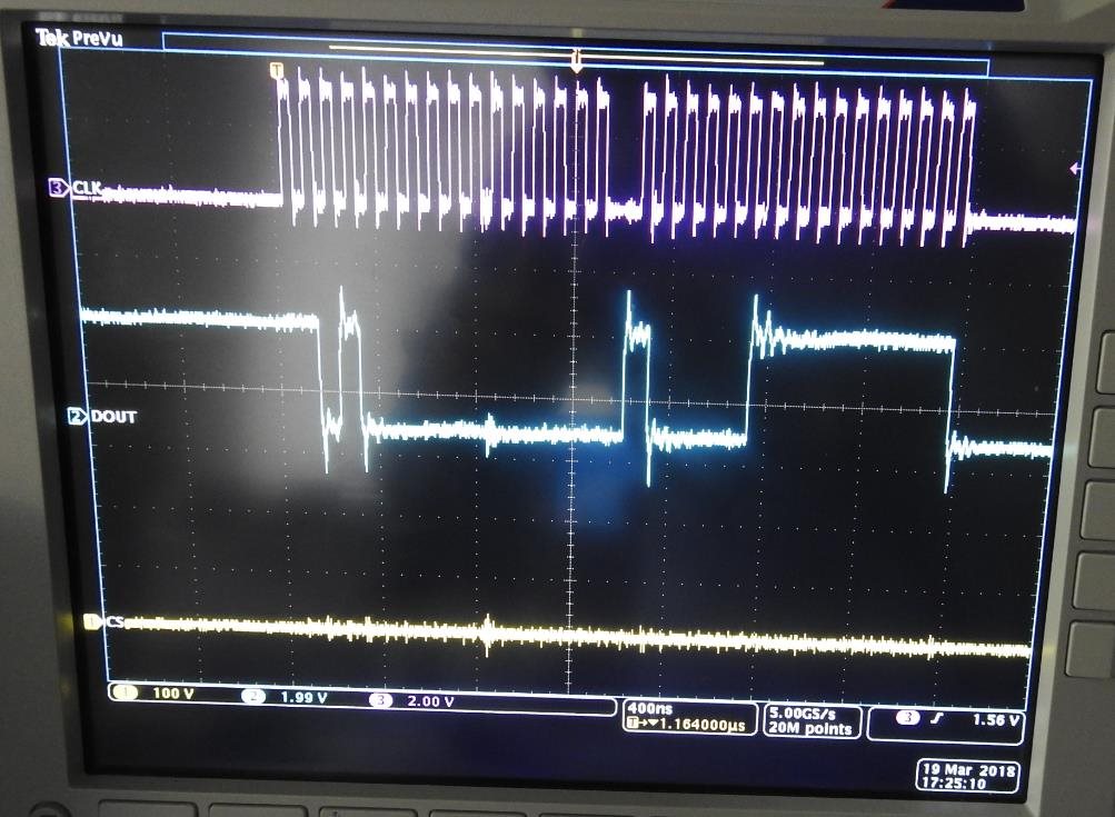
     Can you please let me know what you changed to get correct data? With both D31 and D30 set, you should be able to read out the register content.  You can’t simply set READ_EN without having WRITE_EN set as well.  CONVST will still do a conversion, but with READ_EN set, the output in the next frame will be the register content versus the conversion result. Can you please show a screenshot with a scope for /FS,SCLK, SDI/SDO? Can you tell me what the frequency of your SCLK is?

    Thanks&Regards

    Dale

  • Hi Dale,

    Actually I was not receiving incorrect data earlier. My calculation was wrong. I had to ignore two bits from MSB side but I had ignored from the LSB side. So after correcting the calculation the data was alright.

    Below are the screenshots (second screenshot is zoom’ed version of the first one). DOUT is the signal from Controller to ADC. I could not get an extra Oscilloscope probe to capture DIN, but that signal was zero all the time. The data on DOUT line is: 0xD000_83FF (CR data), 0x0FFF_0FFF (Dummy data to read back the CR)


    Thank you.

  • Hi Gobind,

    I apologized for late response, I was on vacation when you posted update here.

    To be clear, "DOUT" you mentioned is your controller's DOUT and it was connected to ADS8548's SDI pin 22, also you were checking/Reading SDO_A pin 19 for Configuration register contents. Please correct me if my understanding is incorrect.

    There is nothing special for writing and reading the configuration register. When writing 0xC00003FF and then read back - you should get the 0x3FF back. Please refer to other query on E2E as below:

    e2e.ti.com/.../1265127

    After you wrote 0xD000_83FF to ADC,

    1. Were you able to find a clock signal on Pin 34(XCLK)? you set Bit 28 of Configuration register to 1, your writing should work if you can get a conversion clock at this pin 34.

    2. Did you use internal reference to get correct data without any external voltage reference? you set Bit 15 of Configuration register to 1 and this will enable internal voltage source, this is another way to check whether your register writing was successful or not.

    Thanks.

    Best regards

    Dale