This thread has been locked.

If you have a related question, please click the "Ask a related question" button in the top right corner. The newly created question will be automatically linked to this question.

DAC8554: TUE interpretation

Part Number: DAC8554

Hi

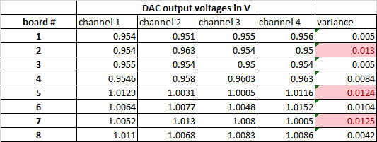
I have 8 different boards (one DAC8554 on each board). I have done the following test:

-set all outputs to 50,000 on all 8 boards.

-Vref used is approx 1.25V on all boards (approx because there are board-to-board variations)

Results are attached

.

According to the DAC8554 datasheet, I have calculated a TUE of 0.971815% of FSR, which is equivalent to 12.1mV if using Vref = 1.25V.

Given this TUE, I would expect the variance between all channels to not exceed the absolute max 12.1mV. However this test shows that 3 out of 8 DACs have their outputs "deviate" upto the marginal values 12 and 13mV...

What am I missing? Is this the way TUE should be interpreted? 

Thank you for your help

Isabelle

  • Hi Isabelle,

    Thank you for your query. I am looking into it. I will get back on this tomorrow.

    Regards,
    Uttam Sahu
    Applications Engineer, Precision DACs
  • Isabelle,

    Just a couple of comments to help expedite things as Uttam looks into this.

    These measurements really should somehow be normalized to the reference values - either that or please provide measured reference values, measured at the same time as the VOUT measurements are taken. The error related to the DAC itself is specified in the datasheet, i.e. assuming a perfect reference, but the measurements you have shared are absolute voltage output values - some error here is contributed by the reference.

    Concerning your TUE calculation I'm not sure I can quite get to what your methodology was in getting to that result. Maybe you can share your calculations etc. to better understand. For older datasheets like this it can be tricky but really we should be looking at the typical specifications for relative accuracy, zero-scale error, and gain error to get an understanding of performance at room. Over temperature the maximum values can be realized given that the top-line condition of the electrical characteristics table states operating temperatures from -40C to 105C.

    Concerning the calculation of variance - I'm not sure how relevant that is given that the datasets are just single-device channel-to-channel variance which is not statistically significant. Datasheet figures would have been based on a larger pool of data, something on the order of 30 units and by proxy 120 channels from multiple lots.
  • Thank you Duke of DACs for your comments. 

    I am working on running this same test again, this time taking note of all ref voltages during the measurement and will get back to you with results today.

    For the TUE calculation, I referred to the calculations discussed in this e2e post: where "0.9718% FSR maximum" is the conclusion for DAC8554.

    I picked variance as a channel-to-channel indicator when I could have simply used the range (=max of outputs - min of outputs). The range is what we usually use for production testing of our outputs accuracy and stability. And so far, this was my attempted way of verifying that outputs are indeed within 0.9718% of FSR.

    Isabelle

  • Isabelle,

    Thanks.

    That post has the correct calculations as I mentioned there. For your tests if you're doing things at room we should mostly be considering the typical specification as I mentioned.

    Let's take a look at your next round of measurements and go from there.

    Thanks.
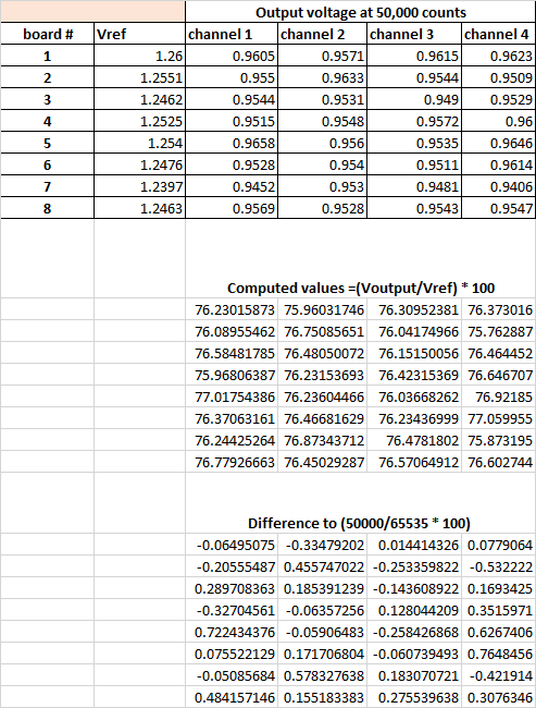
  • Here are the new measurements in the first table:

    The second table are the values "normalized to Vref", formula in title.

    The third table is just playing around with numbers: It is the difference between the second table values and 76.2951094834821 = (50,000/65535) * 100

    Note that the 8 boards are the same as the initial test in my first post, but we have a trimpot that adjusts Vref to match the DAC outputs to our application needs. Hence the DAC output's offset isn't really critical since it can be adjusted by tweaking Vref. Only the channel-to-channel variation is a concern. 

    Thanks

    Isabelle

  • Hi Isabelle,

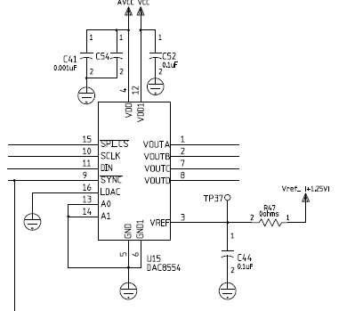
    My apologies for the delay in response. The actual performance will many a time depend on the actual circuit and the measurement. Could you please provide some details on how the measurements are made? Please share the schematics, if possible.

    Regards,
    Uttam
  • I am using a 4 1/2 digit precision multimeter to measure (BK Precision Model 2831E) and two separate fine probes for signal and ground. They are of same length (approx 12").

    I am measuring the DAC output voltages directly from the IC pin:

    Thanks for your help, Uttam.

    Isabelle

  • Hello,

    "Tagging in" once more given the time-zone difference for Uttam.

    Isabelle Guitard said:
    Note that the 8 boards are the same as the initial test in my first post, but we have a trimpot that adjusts Vref to match the DAC outputs to our application needs. Hence the DAC output's offset isn't really critical since it can be adjusted by tweaking Vref. Only the channel-to-channel variation is a concern. 

    Was this trim procedure applied prior to taking this most recent set of measurements? If so, can you describe the exact trim procedure in more detail?

  • Yes, the most recent set of measurements happened post trimpot procedure.

    Vref comes from this LDO and the trimpot is part of a voltage divider on this LDO output pin to set it to  approx 1.25V. 

    The DAC outputs are normally connected to an amplifying stage (op-amp based), and the "trimpot procedure" consists of adjusting Vref to match the desired outputs after amplification.

    However when this last set of measurements was taken, the DAC output pins were floating (disconnected from the op-amp circuitry) so I don't believe the op-amps had an influence.

    Isabelle

  • Isabelle,

    A couple more refinement questions to make sure we understand this completely on our side.

    In the end is the measured VREF value that you've shown in the table the actual VREF value at the time that the VOUT measurements were taken? Or, does the VREF get some tuning yet between the two measurements?

    In this case with the DAC outputs floating, not connected to the amplifiers, how was the trimpot procedure executed? By measurement at the DAC outputs directly? What does the trimpot measurement look like? A measurement at a single code? A two code line of best-fit? Any calculation applied from the measurement to arrive at the appropriate VREF?
  • I hope this detailed procedure clarifies all of your questions:

    Step-by-step procedure for each one of the 8 boards (applies to the last measurements I sent):

    1. Send 32,767 to all 4 outputs

    2. adjust the trimpot while monitoring the 4 amplified output voltages until they all 4 fit in an acceptable voltage window (4.9 V - 5.1 V was the window I used in this case, however I am conducting an analysis to determine how narrow can this window get, hence my very first post asking about how to interpret the TUE so I can better understand what performance to expect from DAC8554 )

    3. Never touch the trimpot again on this board

    4. disconnect the op-amp stage from the DAC output

    5. Send 50,000 to all 4 outputs and measure voltages on the DAC output pins

    Isabelle

  • Isabelle,

    Thank you for your patience and explaining all of this to us. It helps make the full picture much more clear.

    One of the previous questions I would still like clarity on, though I do think I know the answer it remains an important detail, is when the reference is measured in this sequence. I would assume in parallel to step 5? Performing some calibration at a later stage of the circuit could explain why when we look at the DAC itself things are a bit wonky, but my main issue is why the reference:VOUT error calculations would be so bad for so many channels since all we're looking at is the DAC subcircuit accuracy relationship.

    Something else I would discuss is that typically, and this is the case for the DAC at hand, the gain error (and reference error) sources typically dominate the system accuracy. Reference error essentially directly translates to gain error in terms of absolute values but of course not in a calculation normalized to the reference. In gain error calibration typically a two-point line of best fit measurement is performed in order to properly calibrate for gain error as opposed to a single point measurement. If you make a single point measurement it's possible that effects of offset error are "aliasing" into the gain calibration.

    Getting "to the point" with respect to your question - as far as the DAC datasheet goes you can basically consider the specification table as defining the performance of any given channel. You cannot assume any inter-relationship between the channels much the same as you wouldn't assume any relationship between two separate devices. Therefore once you have made the TUE calculation you can assume that another channel could have exactly the opposite polarity of errors, however likely or unlikely that case may be.
  • Hi Isabelle,

    Didi you get a chance to calibrate the gain error in your circuit as Kevin suggested? In case you need to understand definitions of few static parameters in precision DAC, you can go through the following article:

    e2e.ti.com/.../dac-essentials-static-specifications-amp-linearity

    Regards,
    Uttam