This thread has been locked.

If you have a related question, please click the "Ask a related question" button in the top right corner. The newly created question will be automatically linked to this question.

ADS1256: ADS1256 is not outputting the data

Part Number: ADS1256

Hi, 

I have been working on ADS1256 for almost a month now. I am using AVR atmega1284P 8-bit micro-controller. The issue that I am facing is that when I program the ADS, it works for less than 5 seconds and does not work again unless I remove the power and plug it back again. It works for few seconds and then the output disappears again. Please look at my code below, any help is really appreciated. The fCLKIN is 8MHz and SCK is 2MHz. The interrupt function works fine I verified myself. Everything is in the default state and I am reading conversion result at default state. Also, please let me know if my t6 calculations are right. Another thing I want to mention is, I have gaps in SPI clock after every 8 clock cycles. Does this effect the output?

Thanks.

ADS1256.txt
/*
 * ADS1256.cpp
 *
 * Created: 6/13/2018 3:47:12 PM
 * Author : Ajay
 */ 

#include <avr/io.h>
#include <avr/interrupt.h>

#define MYUBRR 51
#define F_CPU 8000000UL
#include <util/delay.h>

unsigned char spi_tranceiver (unsigned char data);
void USART0_Init(void);
void transmit (unsigned char DATA);

int a = 0;
unsigned long adc_val = 0;

ISR(INT0_vect)
{
if (a == 0)
{
	spi_tranceiver(0x03);
	_delay_us(25);
	a = 1;
}	
adc_val = spi_tranceiver(0);
adc_val <<= 8;
adc_val = spi_tranceiver(0);
adc_val <<= 8;
adc_val = spi_tranceiver(0);	
}

int main(void)
{	
	DDRB |= 0b10110000; //Setting the MOSI, SS & SCK as outputs and MISO as input
	
	SPCR |= (1<<SPE)|(0<<DORD)|(1<<MSTR)|(0<<CPOL)|(1<<CPHA)|(1<<SPR0)|(0<<SPR1); //Enabling SPI and setting freq to 2 MH. Also, setting MSB transferred first
	SPSR |= (1<<SPI2X);
	
	EIMSK |= (1<<INT0); //Enables INT0
	EICRA |= (1<<ISC01)|(0<<ISC00); //Interrupt INT0 on falling edge
	
	sei(); //Enable the interrupts
	
    while (1) 
    {
		USART0_Init();	

		transmit((adc_val >>16));
		transmit((adc_val >>8));
		transmit((adc_val));
	}
}

unsigned char spi_tranceiver (unsigned char data)
{
	SPDR = data;
	while(!(SPSR & (1<<SPIF)));
	return(SPDR);
}

void USART0_Init(void)
{
	UBRR0H = (unsigned char)(MYUBRR>>8);
	UBRR0L = (unsigned char)(MYUBRR);
	UCSR0B = (1<<RXEN0)|(1<<TXEN0);
	UCSR0C = (0<<USBS0)|(1<<UCSZ00)|(1<<UCSZ01)|(0<<UCSZ02)|(0<<UMSEL00);
}

void transmit (unsigned char DATA)
{
	while ( !(UCSR0A & (1<<UDRE0)) );
	UDR0 = DATA;
}

/*
 * ADS1256.cpp
 *
 * Created: 6/13/2018 3:47:12 PM
 * Author : Ajay
 */
#include <avr/io.h>
#include <avr/interrupt.h>
#define MYUBRR 51
#define F_CPU 8000000UL
#include <util/delay.h>
unsigned char spi_tranceiver (unsigned char data);
void USART0_Init(void);
void transmit (unsigned char DATA);
int a = 0;
unsigned long adc_val = 0;
ISR(INT0_vect)
{
if (a == 0)
{
 spi_tranceiver(0x03);
 _delay_us(25);
 a = 1;

adc_val = spi_tranceiver(0);
adc_val <<= 8;
adc_val = spi_tranceiver(0);
adc_val <<= 8;
adc_val = spi_tranceiver(0); 
}
int main(void)

 DDRB |= 0b10110000; //Setting the MOSI, SS & SCK as outputs and MISO as input
 
 SPCR |= (1<<SPE)|(0<<DORD)|(1<<MSTR)|(0<<CPOL)|(1<<CPHA)|(1<<SPR0)|(0<<SPR1); //Enabling SPI and setting freq to 2 MH. Also, setting MSB transferred first
 SPSR |= (1<<SPI2X);
 
 EIMSK |= (1<<INT0); //Enables INT0
 EICRA |= (1<<ISC01)|(0<<ISC00); //Interrupt INT0 on falling edge
 
 sei(); //Enable the interrupts
 
    while (1)
    {
  USART0_Init(); 
  transmit((adc_val >>16));
  transmit((adc_val >>8));
  transmit((adc_val));
 }
}
unsigned char spi_tranceiver (unsigned char data)
{
 SPDR = data;
 while(!(SPSR & (1<<SPIF)));
 return(SPDR);
}
void USART0_Init(void)
{
 UBRR0H = (unsigned char)(MYUBRR>>8);
 UBRR0L = (unsigned char)(MYUBRR);
 UCSR0B = (1<<RXEN0)|(1<<TXEN0);
 UCSR0C = (0<<USBS0)|(1<<UCSZ00)|(1<<UCSZ01)|(0<<UCSZ02)|(0<<UMSEL00);
}
void transmit (unsigned char DATA)
{
 while ( !(UCSR0A & (1<<UDRE0)) );
 UDR0 = DATA;
}

  • Hi AjayS,

    Welcome to the TI E2E Forums!

    Are you toggling the /CS pin or just setting it low?
    /CS resets the SPI interface and helps recovery communication if the MCU and ADC should happen to get out of sync, so I would always recommend toggling /CS between SPI commands, if possible, to ensure a clean start to each command.

    I would also recommend programming the ADS1256 to a slower data rate to see if communication improves. By default the ADS1256 is configured for the fastest (30 kSPS) data rate, which might be too fast for the microcontroller to keep up with reading data and transmitting it out the UART. Also, currently you might have only partially transmitted the full 24-bit value through UART when an interrupt occurs (so UART data might appear corrupted).


    You might also have a look at this similar E2E thread: e2e.ti.com/.../2602393. A lot of the recommendations I gave to troubleshoot that issue would apply to this as well; particularly checking to see if perhaps there is a signal integrity issue on the SPI bus that might cause the ADC to stop responding to commands.

    Best regards,
    Chris

  • Hi,

    The CS pin is always low. I am sending the SYNC command as well but it still does the same. If I lower the SPI frequency to 1MHz, something strange happens. The SPI 32 clocks won't fit into the DRDY one cycle. Meaning the DRDY goes high again before all the 24 bits are shifted out.
    I was also trying to program it but I am having issues. The WREG command is straight forward which is 0x50. So when the DRDY occurs, I send 0x50, followed by the register address which is lets say 0x00 (status register). What I don't know is the I/O command that I am supposed to send after register address. The last byte would be the data for the register I want to write. So, is it okay to write like:

    spi_transreceiver(0x50);
    spi_transreceiver(0x00);
    spi_transreceiver(??);
    spi_transreceiver(0x00);

    I was also looking at the Arduino code for this ADS1256. I tried the same thing but cannot get it working.
    Thanks.
  • Hi AjayS,

    For the WREG command, the command byte (0x50) and the register address should be AND'ed together... Therefore, in your example the command to write, starting at the STATUS register, would be "0x50". (To write to the MUX register, address "0x01", the command would be "0x51".)

    To write to a single register then, you'd only need to send 3 command bytes: "0x50 0x00 0x??", where the first byte is the command byte/address, the second byte is the number of registers to write to (-1, such 0x00 writes to a single register, and 0x01 writes to 2 registers, etc.), and finally the third byte is the data you want to program.

    Writing to the DRATE register to reduce the ADC's data rate, would look like "0x53 0x00 0x03", where "0x03" corresponds to 2.5 SPS.
    Try sending this byte sequence, and then checking if the /DRDY pulse period is reduced to 1/2.5 SPS, or a pulse every 400 ms.

    Best regards,
    Chris
  • Hi Chris, 

    I have tried giving the 0x50, 0x00, 0x03 but the DRDY pulse is always the same which is 64us no matter what value of the SPS I give in. It means that there is something wrong with the code. So, the way I have it is as below:

    a=0;

    ISR(INT0_vect)
    {
     if (a == 0)
     {
     spi_tranceiver(0x50);
     spi_tranceiver(0x00);
     spi_tranceiver(0x03);
     _delay_us(5);
     a = 1;  
     }
     
     else
     {
     spi_tranceiver(0x01);
     spi_tranceiver(0x00);
     spi_tranceiver(0x00);
     spi_tranceiver(0x00);
     }
    }

    I am not really sure other ways to do it.

    Thank you for helping,

  • Hi AjayS,

    I might recommend first sending the RESET command before first trying to configure the device. RESET might help alleviate any potential start-up issues and it also puts the device in SDATAC mode (which allows you to write to the device registers).

    If that doesn't resolve the issue, would you able able to capture an oscilloscope screenshot of your SPI communication and share it here (specifically of the WREG command bytes)? ...Often times you can spot communication issues on an oscilloscope that you wouldn't know about from only looking at the code.

    Best regards,
    Chris
  • Hello Chris,

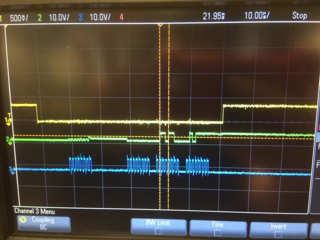
    So, I played around with the ADS1256 a little bit and turns out that I did program it to sample at 2.5SPS. I wasn't zooming out on the oscilloscope to see 400ms. I had scale set to 50us and that's why I was missing the entire waveform. Also, I have tried the different commands for different SPS and it all worked out. The next issue that I am encountering is the output bits. For example, the output at maximum negative input should be 800000h but its not. Same for exact 0. The output does corresponds to the input and changes when I change the input but it is different that what it should be. I have attached the waveform picture below:

    The blue wave is the SPI clock, the yellow is the DRDY and the green is the output. The input is ground to both the channels.

    Thanks again 

  • Hi AjayS,

    I'm glad to hear that you've made progress on the communication issue!

    How far off is the ADC's output result from the input signal? Would you be able to provide some examples?

    You'll want to check if the offset and gain error can be explained by the specified errors of either the ADC or the signal source. Also, look at the reference voltage and make sure that it is accurate and not oscillating. Any errors in the reference source will directly affect the ADC output result.

    Best regards,
    Chris
  • I have never touched the offset or calibration of the ADS1256 and I am not really sure if that's the problem here. The way I have configured the ADS1256 connections are:

    VREFP = 5.0V
    VREFN = 0.0V
    ACOM = 0.0V
    AIN0 = either 0V or 5V
    AIN1 = 0.0V

    I am using AIN0 as my positive channel and AIN1 as negative. When I have 0.0V at AIN0, the output is 0b00000000 00111000 0110100. And when I have 5.0V at AIN0, I get 0b01000000 10000110 01000110. This seems to be the same even if I use different channels. For the power supply, I have a smooth DC input (checked on oscilloscope). I tried doing the offset and gain calibration, nothing happened.

    Many thanks,
    Ajay
  • Hi AjayS,

    Try reducing the voltage on VREFP to 2.5V...

    The ADS1256 isn't meant to be used with a reference voltage greater than 2.6V. This larger voltage might be causing some internal leakage or other undesirable effects that could be affecting the conversion result.

    Best regards,
    Chris
  • Hi Chris,

    I have changed the VREFP to 2.5V but the result is still the same. Do you think I may have damaged the IC by putting in 5V to the VREFP? I have tried multiple things and I cannot get exact 0 at 0V. There is always some 1s in the result. Is there anything else that I am missing that causing this?

    Thanks a lot for your help.
  • Hi AjayS,

    I don't think that would have damaged the device since it does not exceed the "abs. max" specification.

    Again, how close to "0" are you getting? With a 24-bit ADC it's quite unlike that you'll get to an exact code, since one code is a very tiny step size. If you're within +/- 100 codes, you're probably just seeing an offset. Also keep in mind that the output is signed, so 0xFFFFF (-1) is a likely output around 0V.

    Best regards,
    Chris
  • The ADS1256 is working completely fine now. Thanks Chris. I unplugged; and plugged the power back in to the ADS1256 and it works. Now I get 7FFFFFh when the positive input is max and 800000h when the negative input is max. Thank you Chris and TI, I love y'all.