This thread has been locked.

If you have a related question, please click the "Ask a related question" button in the top right corner. The newly created question will be automatically linked to this question.

ADS7844: SPI DOUT producing undocumented output

Part Number: ADS7844

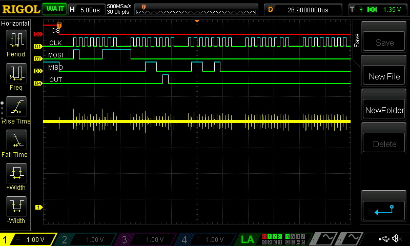
I have ADS7844 ADC IC and experiencing some strange data from the device. The current device setup is:

  • Vcc - +3.3V
  • COM - GND
  • Vref - +3.3V
  • SPI Clock - 160kHz
  • CH_0 - +3.3V

As you can see the 1st byte on the MOSI line is the Control Byte starting with the high bit. I am requesting conversion for CH_0, so the following bits are 0, 1 low bit as per datasheet. Following that a single HIGH bit to denote SINGLE-ENDED mode, then the last 2 bits as HIGH to keep the device powered up.

What I am expecting after that as described in the datasheet is the BUSY signal to be HIGH (between the 1st and 2nd bytes). What actually happens the ADC IC responds with a constant value of 0x18h in the 2nd byte and then the bytes 3 and 4 contain the voltage value. 

The datasheet describes that after the 1st byte the MSB of the analogue reading will be transmitted.

I cannot find any information in the datasheet that would describe the response on the MISO line to be in 3 bytes. I am not using daisy chaining. I've tried restarting the device, the issue persists.

Any help would be much appreciated.

Thanks.

  • I am adding an edit as a reply.

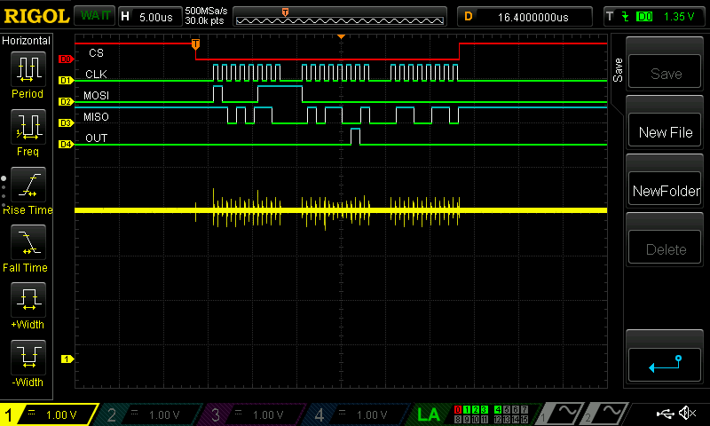
    I've optimised the SPI transmission, however the traces are still providing strange data from the ADS7844 IC.

    So now, I am sending only 3 bytes - 24 SPI Clock Cycles. Still CH_0. As you can see the Control Byte is the same. The ADC IC does not provide the BUSY signal until almost the end of the second byte. Should I wait until it the BUSY goes low and then send the second and 3rd bytes?

    Also the last byte received from the IC, never has the last 4 bits as 0s.

  • Hello,
    Would you please clarify what the signal named OUT represents? Is this the BUSY signal ?
    It seems the MISO communications are correct, the next thing to look at are the timing requirements of the device and making sure there are no timing violations. Is the Aquire time after the fifth clock pulse (bit3) of the control byte long enough, min of 1.5uS?

    Regards, Cynthia
  • Hi Cynthia,

    Thank you for your response. I have some updates since I created the post. First - I have noticed that the COM and SHDN pins were wired the wrong way. I had COM to Vcc and SHDN to GND. I am surprised the device even worked.

    Now I have COM wired to GND and SHDN to Vcc. I have made slight changes to other pins too. The device is powered from +5V (Vcc), and the Vref is +3.3V - do you know any reason why this would not be ok?

    Since I have made chose changes, the device does not respond at all. Maybe it gone bust due to incorrect wiring earlier? 

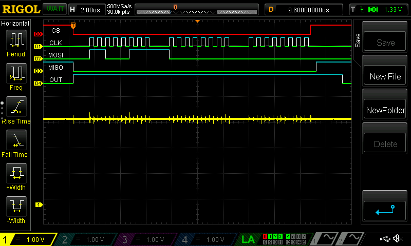
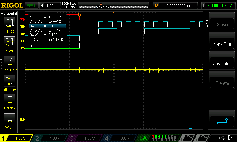
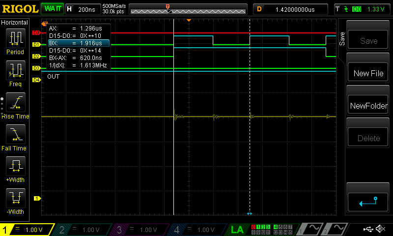
    Please see the most recent trace below. As you may notice the control byte is now requesting channel 1 which is 0x40. The OUT (BUSY) line is pulled high by the ADC device but never goes low. The BUSY pin on the ADC IC is not connected to anything.

    The Yellow analogue trace is the CH_1 voltage supplied to the ADC IC pin 2.

    Because the OUT (BUSY) signal does not go LOW I can only time it to the next byte. There are 3.4us between the end of the 5th Clock Pulse and the next byte.

    SPI bus is configured at 1.6MHz speed. This should give a 100kPS.

    Thank you.

  • That is good, I am glad those connections have been fixed. But you might be right that the device has been damaged and will no longer work correctly. Could you switch out to a good device for future testing?
    As for having Vcc = 5v and Vref=3.3V there should not be anything wrong with this, just note that Vref determines the analog input range, meaning 3.3V.

    I see from your shot after CS goes high, that BUSY stays high and then changes states. This should not be the case.
    Could you restart the device and give it a CS pulse, if BUSY goes high at the falling edge of CS again, wait until BUSY goes low to release CS. After that try to communicate to the device normaly and see if it response correctly. I do believe this device is damaged though.
    Regards
    Cynthia
  • Hi Cynthia,

    Thank you for your response. I tried on two different ICs - and both have been wired incorrectly. Both produced the same traces with the BUSY line always going HIGH and never falling. I do not have any additional ICs left, so will have to wait until I get more and try again.

    Thanks for your help.

    Kind regards,

    Dainius