This thread has been locked.

If you have a related question, please click the "Ask a related question" button in the top right corner. The newly created question will be automatically linked to this question.

ADS1299: ADS1299: Testing bias / Right-leg drive

Other Parts Discussed in Thread: ADS1299, TINA-TI

Hi,

This is a continuation on the thread here (https://e2e.ti.com/support/data_converters/precision_data_converters/f/73/t/696153). previously suggested a scheme to test RLD with ADS1299, which I finally got a chance to test out.

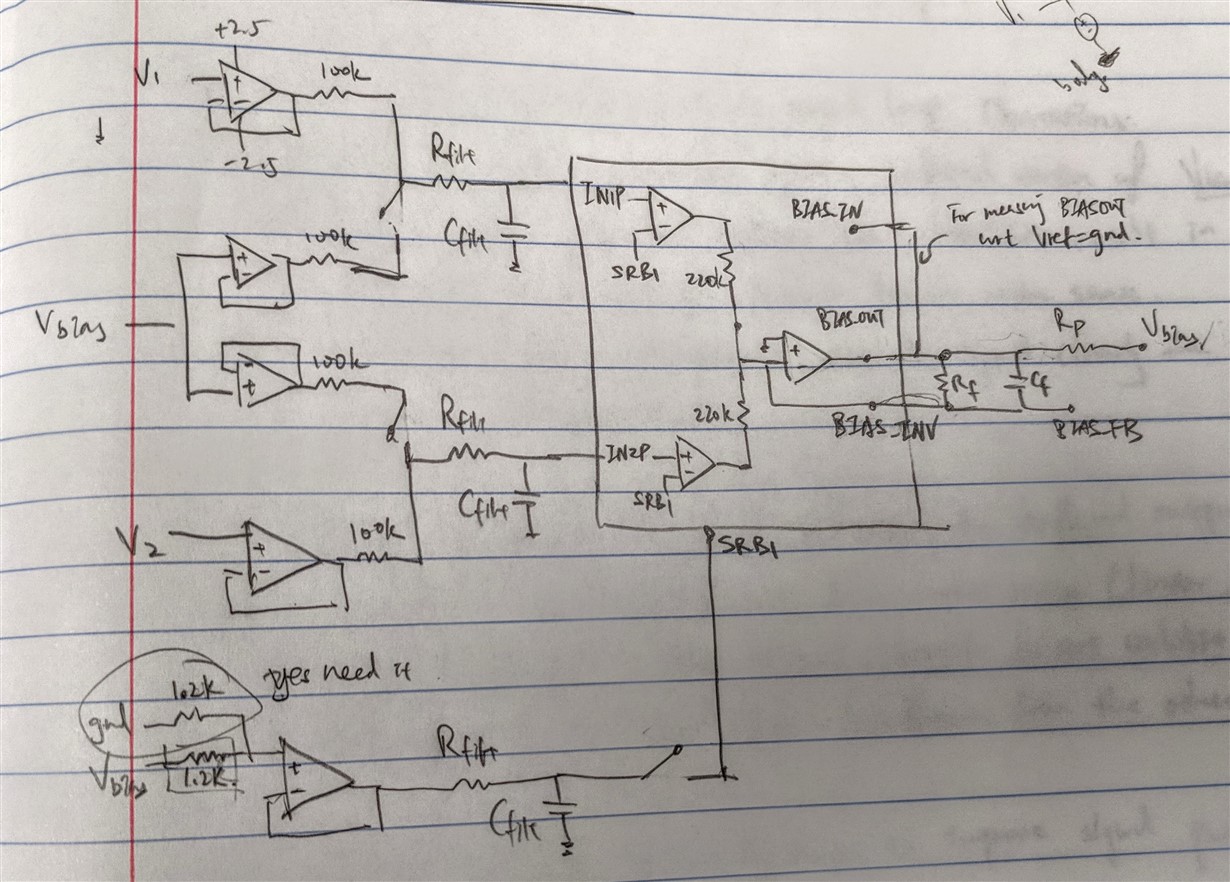
My test results are a bit confusing, I'm hoping to check if what I got is expected. Below is the my final test setup for RLD (same as the last one suggested in the linked thread). The test signals V1 and V2 are square waves generated by a raspberry pi and attenuated by voltage dividers.

The big box represent the ADS1299 chip.

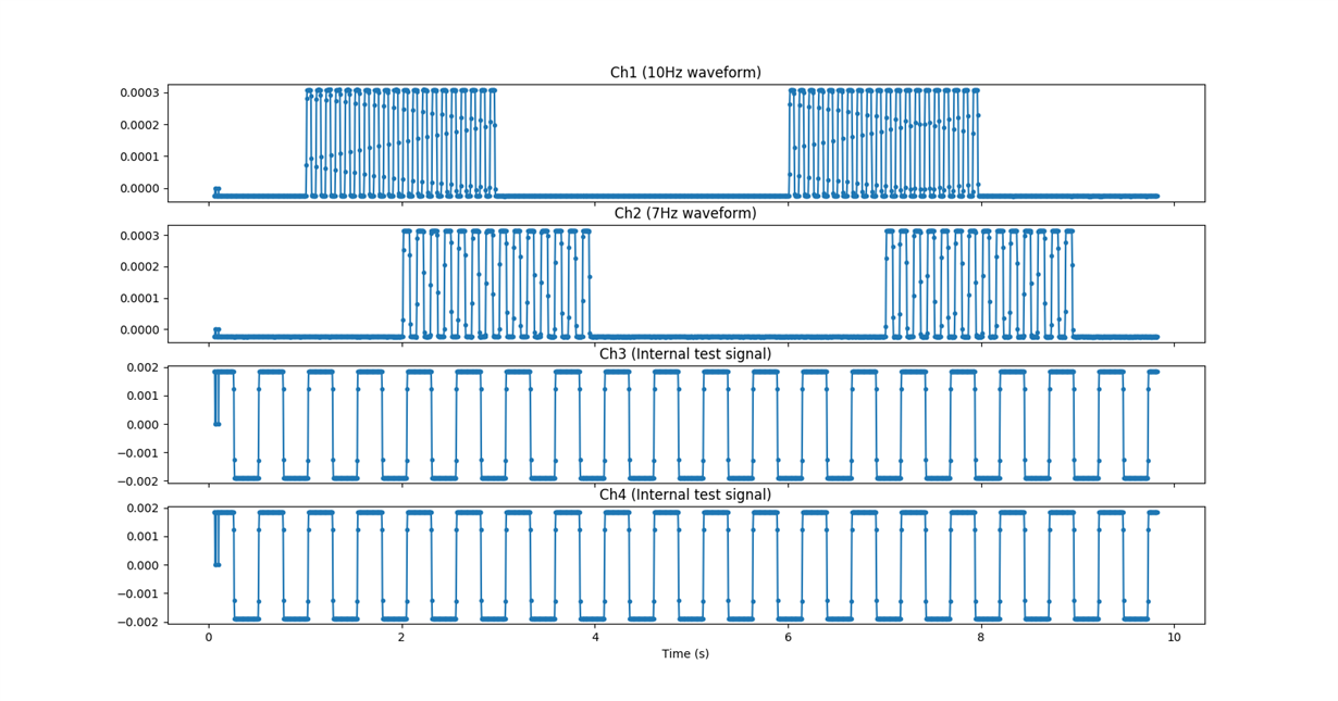
Test 1: The bias amplifier is turned off. V1 and V2 are fed directly to Rfilt, the op-amp summers were not used in this test.

             Ground (equal to average of VSSA and VDDA, and V1 and V2 signals are generated with respect to this voltage level) is fed into SRB1 directly. This is my baseline measurement.

            Ch1 and Ch2 show clean square waves of  0.3mV as expected (vertical axis is in volts). The temporal delays are as correct. Ch3 and Ch4 are internally generated signals. Everything looks good.

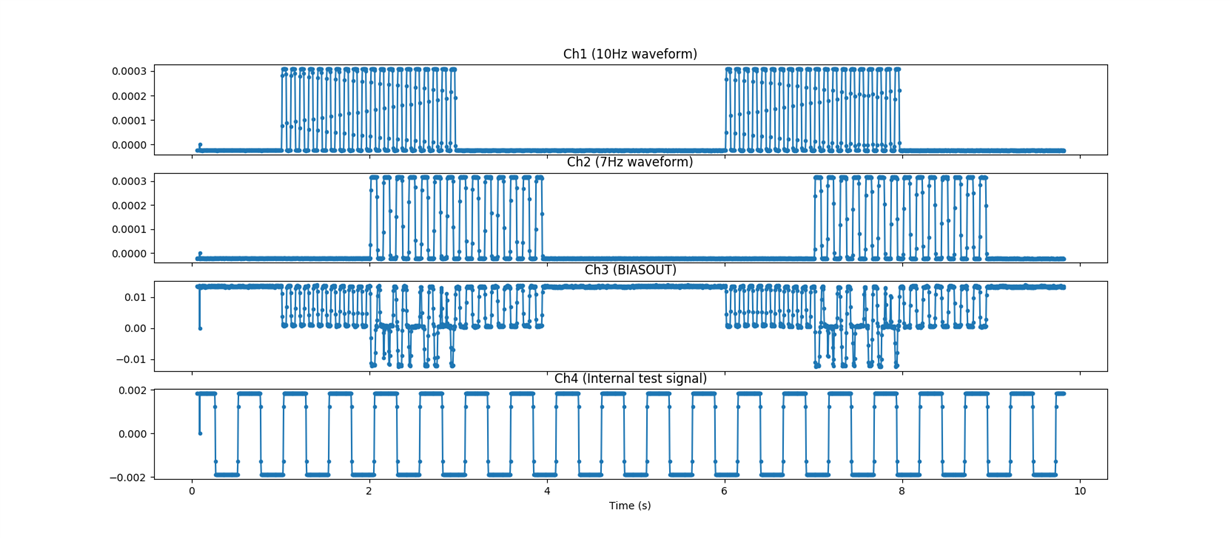
Test 2:  Ch1 and Ch2 are as before. Now BIASOUT and BIASIN are connected and routed to IN3P. BIAS_SENSP are configured such that IN1P and IN2P are routed to the bias amplifier to produce averaged common mode, which is applied on BIASOUT pin. Because the feedback loop is open, we see Ch1 and Ch2 signals are unaffected.


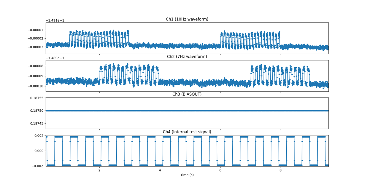
Test 3:  Here we close the RLD feedback loop. Buffered V1 and V2 are summed with buffered version of Vbias before reaching IN1P and IN2P.  Buffered Vbias instead of ground is fed into SRB1. The resulting signals are shown below. Ch1 and Ch2 are now severely attenuated and the square waves are about 20uV peak-to-peak. However, the BIASOUT measured on Ch3 is perfectly flat.

               This doesn't make too much sense..

Test 4: In the final test, Vbias and ground is summed together, and the summer's output is applied to SRB1. The resulting Ch1 and Ch2 are noisier and shows some interference from the other channel.

            However, the amplitude of Ch1 and Ch2 are not attenuated as much (0.2mV peak-to-peak, which is more reasonable). Ch3 shows BIASOUT that looks like the average of Ch1 and Ch2.

 So my questions are: While test 3 shows cleaner measured signals, why would BIASOUT flat in test 3? Is this expected?

I think test 4 is a closer simulation of what happens during actual EEG measurement, i.e. the potential on the ground electrode is affected by the bias drive. But in this case, what can be done to minimize the inter-channel interference due to the common-mode extraction by averaging? I think changing the Vbias+V1 or Vbias+V2 summer resistors can tune this behavior, but this is hardly controllable during actual EEG usage.

  • Hi Allen,

    Thanks for your post, and please excuse our delay.

    The BIASOUT signal in Test 3 looks like it is clamped to a positive full-scale output. Assuming a 4.5-V reference voltage (VREFP - VREFN) and PGA = 24 V/V, the maximum differential input voltage to the PGA on each channel is +/-4.5 / 24 = +/-187.5 mV.

    I don't see anything wrong with your setup in any of the tests. Remember that measuring the BIASOUT signal through BIASIN will disconnect the PGA on that channel from the SRB1 inputs. The output of Channel 3 will be (BIASOUT - BIASIN) X PGA.

    How are you routing the signals for BIAS measurement? Are you shorting BIASOUT to BIASIN and setting the Channel 3 MUX to 010 (CH3SET[2:0] = 010)? Or are you routing both BIASOUT and BIASREF to the normal Channel 3 input pins? If you could share the register settings for Test 3, that would be helpful.

    I would suggest that you try simulating your experiments using the free TINA-TI spice simulator. You could use the ideal op-amp models and a pair of function generators to measure the effects of the BIAS drive circuit.


    Best Regards,

  • Ah you are right that BIASOUT signal in Test 3 is clamped. Re routing the signals for BIAS measurement, I did short BIASOUT to BIASIN and set CH3SET[2:0]=010. Is the BIASOUT signal the expected behavior given these settings? I'm having trouble getting my head around this.

    Re TINA-TI...is this just regular SPICE sim, or does it have special TI models?

    Finally, these test results seem to suggest that introducing BIAS drive doesn't necessarily improve the signal quality...is this a strategy that should be used on a case-by-case basis?

  • I think you're BIASOUT signal output looks correct given the measurement settings. The output of Channel 3 will be the difference between BIASOUT and the BIASREF voltage times the PGA gain. This would effectively be the same as viewing the output with an oscilloscope probe on BIASOUT and AC-coupling the scope channel to remove the DC content.

    TINA is just our own SPICE simulator developed by a third-party company. Many of our analog devices are released with TINA models that include performance parameters from the device datasheet. For the purpose of modeling the BIAS circuitry, ideal op-amps could be used.

    Deriving an average of the input electrodes and driving the inverse of that average back to the subject is a proven technique for reducing common-mode noise in biopotential applications. It may take some adjustments based on your application. Start with a DC bias voltage only (i.e. BIAS_SENSx = 0x00) and select individual electrodes as needed to derive the AC common-mode.

    Check out this app note below. It describes the use of right-leg drive (RLD) in ECG systems, but the concept is exactly the same.

    www.ti.com/.../litabsmultiplefilelist.tsp


    Best Regards,