Other Parts Discussed in Thread: TLE2027
Hello
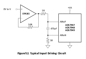
I, like dale, am using a ADS7947 ADC. It is being used to replace an obsolete ADC (from another manufacturer) in some existing equipment. One of the requirements is that I should make as few changes to the existing circuits as possible. The example on page 27 of the datasheet looks this:
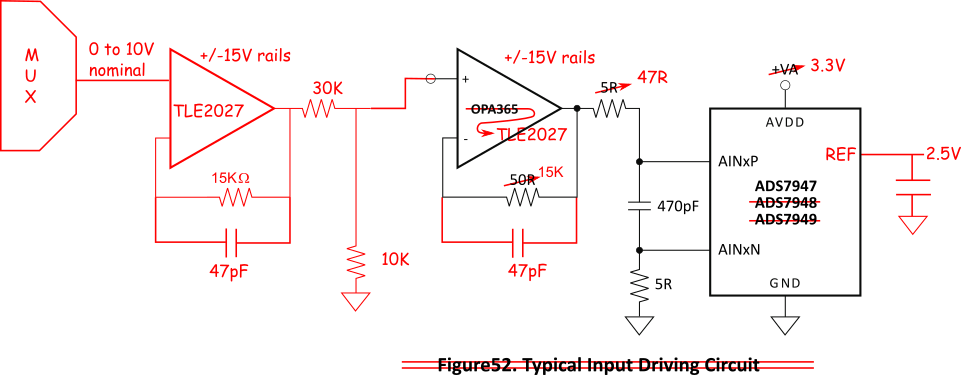
The modified circuit with the new ADC in our equipment looks like this:
I didn't want to change the driving op-amps because we wanted minimal changes. This is just a design, it hasn't been be sent out for manufacture, or even prototyped.
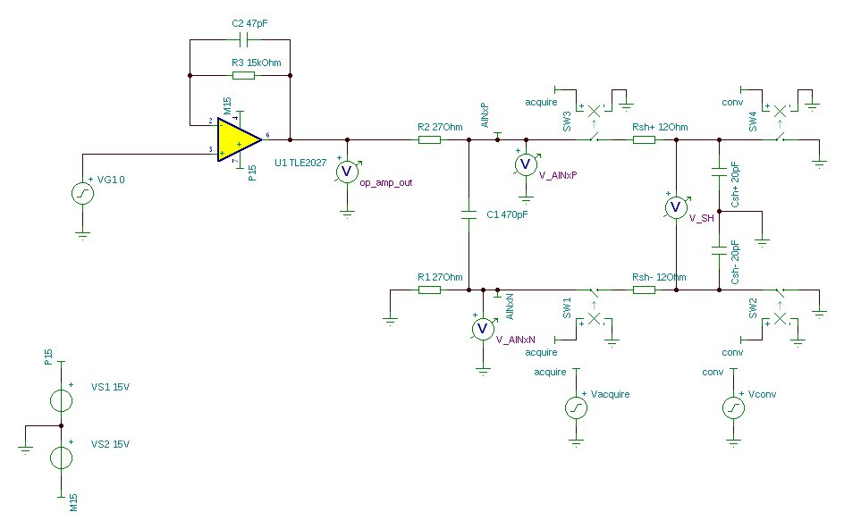
The TLE2027 op-amps are what is used in the existing product. I did a spice simulation and found that the TLE2027 nearest the ADC wasn’t able to drive a load consisting of the 5R + 470pF +5R in series without the op-amp ringing. Changing the upper resistor to 47R made the op-amp output stop ringing and ADC input settle in the minimum time (according to the spice model). The slew rate of the leftmost TLE2027 is horrible (1V/us worst case) and mostly determines the settling time of the signal at the ADC but we can live with that because our sample rate is very low (about 28us per sample). (switching time of MUX + 13.5V * / 1V per us << 28us)
However there is some advice in the datasheet page 27 that reads:
It is recommended to split the series resistance of the input filter in two equal values as shown in Figure 52. It is recommended that both input terminals see the same impedance from the external circuit.
This suggests that the circuit should be changed so that we have 27R + 470pF +27R in the filter before the ADC
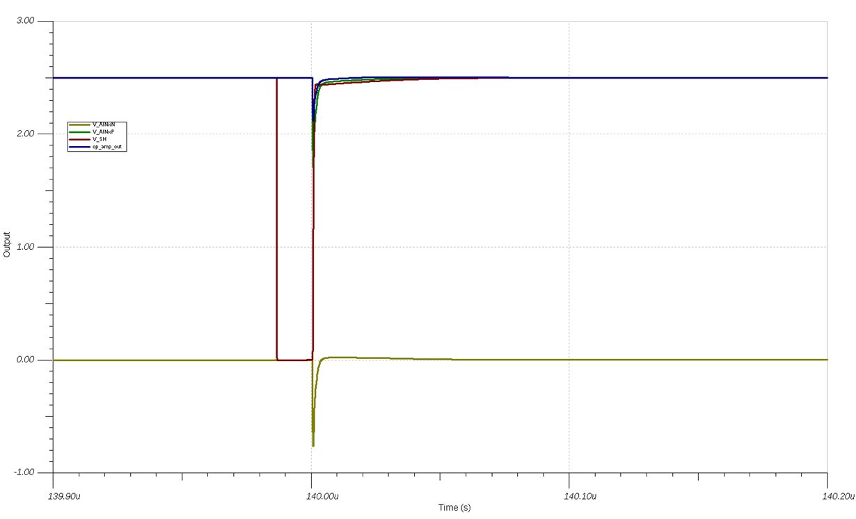
But the datasheet also says that the ADC inputs are pseudo differential and that the voltage on the AINxN pin should vary by more than +/-200mV with respect to GND. If I have an 27R resistor on the on the bottom of the input filter in front of the ADC, then the AINxN pin gets a bigger transient on it that lasts for longer before settling (in the spice model). The transient on AINxN is smaller with the 5R resistor.
Also page 28 of the datasheet shows a range of different resistor values used in the input filter, but the bottom resistor is a constant 5R.
My question: which is the better selection of component values to use?
-
47R + 470pF + 5R ?
-
27R + 470pF + 27R ?
Is it OK for the AINxN pin to briefly go outside the +/-200mV range when the acquisition starts?
If the sample time is 28 us, am I worrying about the resistor values unnecessarily?


