This thread has been locked.

If you have a related question, please click the "Ask a related question" button in the top right corner. The newly created question will be automatically linked to this question.

AMC1304L25: gain error when sensing voltage : front end question

Part Number: AMC1304L25
Other Parts Discussed in Thread: AMC1210

Hi everybody,

I'm using AMC1304L25 to measure DC+AC voltage, up to approx. 250V. Thus using large voltage resistor divider.

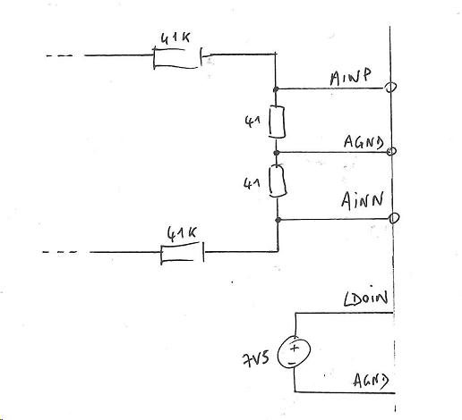
I designed a fully symetrical input stage to cope with issue described in section 9.2.2 of the datasheet.

I mean the sensing resistor is splitted in two and the middle point connected to AGND. This is slightly different from figure 56 of the datasheet.

But we are getting approximately -2.2% of error (measured at different voltage levels). Apparently a gain error.

Is it the right thing to do ?

thanks and regards,

Alain

  • Hi Alain,

    Welcome to our e2e forum! If you tried to attach a file with your AMC1304L25 query, unfortunately it did not come through. Having a large shunt can impact the gain error of your circuit. Have you taken a look at the application note written a couple years ago by one of my colleagues Polly Chung? You can find it here: www.ti.com/.../sbaa214.pdf - you may find some of her testing useful in your application.

  • Hi Tom,

    Thanks for answering.

    Yes, I had a look at this note.

    I'm using a rather low shunt value (2*41.2ohms) to keep gain error under control (about 0.3% as far as I understand).

    I was then surprised of getting a final error of about 2.2%.

    See below schematic. Am I wrong ?

  • Hi Alain,

    The sketch seems OK, what are you using for the digital filter on the AMC1304L25 output?
  • Hi Tom,

    We are using AMC1210 as stream demodulator.

    With below settings

    AMC1210 clk is 10 MHz.

     Filter_CTRL :      0x4

      • Pin CLKx is an input
      • Signal SH2 is chosen as sample-and-hold signal
      • The time is measured from the last filter update to the last rising edge of the selected sample-and-hold signal
      • The clock speed is equal to the data rate from the modulator
    • Filter_SYNC :      0xFF9
    • Sinc filter runs with a Sinc3 structure
    • The acknowledge flag is enabled for the particular filter
    • The filter is enabled and data are produced in the sinc filter and/or integrator
    • Oversampling ratio = 250 (0xF9+1)
    • Filter_INT   :       0x4800
    • Shift control = 9
    • The data is stored in 16-bit two's complement
    • The demodulation for resolver applications is disabled
    • The data from the sinc filter output is stored in the register map
    • The oversampling mode updates the data output of the integrator
    • Oversampling ratio = 1 (0x0+1)
    • Filter_COMP :   0x0
    • The modulator failure flag as well as the output INT is disabled for this particular flag
    • Comparator filter runs with a sincfast structure
    • The low-level interrupt flag as well as the output INT is disabled for this particular flag
    • The high-level interrupt flag as well as the output INT is disabled for this particular flag
    • Oversampling ratio = 1 (0x0+1)
    • General_CTRL : 0x0
    • New data is signaled with a '1' on the pin ACK
    • An interrupt is signaled with a positive transition on the pin INT
    • Interrupt pin and interrupt flags are blocked (interrupt pin INT always inactive).
    • Pattern count = 0
    • Clock_DIVIDER : 0x800
    • The high current option for pins PWM1 and PWM2 is disabled
    • Sinc filter units can be enabled if bit FEN is '1'.
    • Signal generator is disabled
    • No phase calibration is performing
    • Clock divider is off, outgoing clock equals incoming clock

    Thus, we assume a full scale range of OSR^3 / 2^shift_control (ADC code) = 205^3 / 2^9 = +/-30517, corresponding to the analog input range (+/-312.5mV)

  • Hi Alain,

    Everything looks OK here, I curious, how are you getting the LVDS signal to/from the AMC1304L25 to the AMC1210?
  • Hi Tom,

    Sorry for late answer (vacation).

    Problem is not the LVDS signalling.

    I'm not proud to say that, after investigations, we found that the bridge resistor values (high voltage side) were not correct/expected values.

    After correction, the final error is less than 1%.

    I think we can close this topic.

    Thanks for your help

    regards,

    Alain

  • Hi Alan,

    Thank you for getting back to us!  I'm glad to hear that the issue is resolved!