This thread has been locked.

If you have a related question, please click the "Ask a related question" button in the top right corner. The newly created question will be automatically linked to this question.

[VC5503] Confirm the release timing of nRESET pin

Guru 24520 points

Hi TI Experts,

Please let me confirm the following question.

[Question]
According to the datasheet, the nRESET pin release timing is R3 + R2 duration time.
Does the "CLKOUT" mean the actual pin?
My customer said that the CLKOUT output was not generated during reset pin hold low. After releasing this pin, the CLKOUT was generated the signal. This is why they would like to know whether the CLKOUT description in Figure5-16 on datasheet is actually pin or not.

And can this device output the CLKOUT signal before releasing the nRESET pin?

Also, the following pin during nReset hold low was the following pin status.
EMU0/nOFF: High
EMU1: High
nTRST: Low

If you have any questions, please let me know.

Best regards.
Kaka

  • Hi Kaka-san,


    Below is my answers to your Questions.


    Q1. Does the "CLKOUT" mean the actual pin?


    Yes, CLKOUT is a DSP clock output signal. CLKOUT cycles at the machine-cycle rate of the CPU. CLKOUT goes into high-impedance state when OFF is low.


    Q2. Can this device output the CLKOUT signal before releasing the nRESET pin?


    Below is the explanation of clock generator during reset.


    Clock Generator During Reset - The DSP can make use of the output clock signal during reset. While the DSP reset signal is held low:


    • The clock generator is in the bypass mode.

    • The output clock frequency is determined by the level of the signal on the CLKMD input pin:


    CLKMD Signal Output Frequency

    • Low - Input frequency
    • High - 1/2 x Input frequency

    CLKOUT bit in the EBSR defaults to zero (during reset) which means clock out is enabled.


    Could you clarify on my below questions.


    • What is the input clock source ? Since you are referring to (R3+R2) delay during reset, my assumption is that customer is not using internal oscillator.
    • Also I hope R2 timings taken care ?
    • Could you also confirm on EMU1/nOFF , EMU0 and nTRST signal status again, you had mentioned EMU0/nOFF I think it’s a typo..it should be EMU1  -  When TRST is driven low, EMU1/OFF is configured as OFF. The EMU1/OFF signal, when active-low, puts all output drivers into the high-impedance state. Suspect if this is taken care correctly?


    Regards

     Vasanth

  • Hi Vasanth,

    Thank you for your response.
    This is not my first question, but I checked the datasheet and some user's guides, but I could not find "CLKMD" input pin. What is this?
    It seems that the"CLKMD" is register name.

    Also I answered your questions as below.
    What is the input clock source ? Since you are referring to (R3+R2) delay during reset, my assumption is that customer is not using internal oscillator.Also I hope R2 timings taken care ?
    [Kaka]
    They used the 24MHz external oscillator for VC5503. This is why my customer need to take care of "R2" parameter.

    Could you also confirm on EMU1/nOFF , EMU0 and nTRST signal status again, you had mentioned EMU0/nOFF I think it’s a typo..it should be EMU1 - When TRST is driven low, EMU1/OFF is configured as OFF. The EMU1/OFF signal, when active-low, puts all output drivers into the high-impedance state. Suspect if this is taken care correctly?
    [Kaka]
    I apologized for confusing of you. There is a typo on my previous post.
    EMU0: High( pull-up with 4.7k ohms)
    EMU1/nOFF: High(pull-up with 4.7k ohms)
    nTRST: Low(pull-down with 10k ohms)
    I could share the schematics with you if you teach me your Email address. If possible, would you please check this?

    Best regards.
    Kaka

  • HI Kaka-san,

    Can you further delay the reset de-assertion period and check ?

    Is it possible to provide the oscilloscope snapshot including reset, clock input, clock out and the other EMU related signals.

    Regards

     Vasanth

  • Hi Vasanth,

    I got some oscilloscope snapshots from my customer. I attached this to this post. please check this.

    snapshot.pdf

    First slide is captured the following signals.
    CH1:EMU1/OFF
    CH2: nTRST
    CH3: CLKOUT
    CH4: nRESET
    Second slide is captured the following signals.
    CH1:CLKIN
    CH2: CLKOUT
    CH3: nRESET
    CH4: DVDD
    Last slide is captured the following signals.
    CH1:CLKOUT
    CH2: nRESET
    CH3: DVDD
    CH4: CVDD

    If you have any questions or need more information, please let me know.
    Best regards.
    Kaka

  • Hi Kaka-san,

    Thanks for sharing the snapshots. At least from my initial parsing, I see that EMU signals are driven as expected.

    Could you please also reply to my other questions.

    • Can you further delay the reset de-assertion period and check clock out pin ?
    • What would be the consequence of clock out not generating before reset getting released in your application ?

    With respect to schematic review, since this is an older device I do not think it would be possible to review the schematics.

    Regards

     Vasanth

  • Hi Vasanth,

    I got more feedback from my customer. Please see the following attached documents.
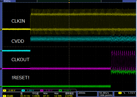
    I think that it can answer to your questions. Also I requested them to check whether if the reset signal transitioned from High to low with generating CLKOUT, the CLKOUT will keep to generate the clkout. As a result, VC5503 stopped the clkout signal.

    snapshot_2.pdf
    If possible, would you please confirm whether the CLKOUT will generate the signal during reset with using your EVM(VC5509A)? We do not have this evaluation board.

    If you have more questions, please let me know.
    Best regards.
    Kaka
  • Hi Vasanth,

    I am waiting for your feedback.

    Best regards.
    Kaka
  • Hi Kaka-san,

    From the snapshot you shared it seems like the clock out is dependent on reset, but wasn't clear on how long reset was held low.

    Could you pl let me know on my below questions:

    1. Could you explain how the pins X1 and X2/CLKIN are handled ?

    2. What would be the consequence of clock out not generating clock before reset getting released in your application ?

    3. How long was the reset held in low ? Can you further delay the reset de-assertion period and check clock out pin ?

    Also, As suggested by you I looked into DSK C5509A. But in DSK since the internal oscillator it wouldn't be possible to check on this scenario. As per datasheet, If internal oscillator is used then the oscillator is always enabled following a device reset and that's what has been observed as well. EVM has external crystal connected between X1 and X2.

    Regards

     Vasanth

  • Hi Vasanth,

    I answer your questions as below.
    1. Could you explain how the pins X1 and X2/CLKIN are handled ?
    X1 pin is floating.
    X2/CLKIN pin is connected to the 24MHz external oscillator as close as possible to device.

    Please let me confirm the background of Question No.2, No.3.
    I need to confirm whether the VC5503 will work even though the clock out was not generating clock before reset getting released. Is this correct?
    For No3, I need to confirm whether VC5503 will generate the CLKOUT if the reset signal keep the Low. Is this right?


    Best regards.
    Kaka

  • Hi Kaka-san,

    To clarify further,

    On Q 2:

    Would like to know what is an impact on the application if clock out is not generated during reset.

    On Q3.

    Yes your understanding is correct, Would like to know the state of clock out, if the reset is held low for further duration.

    Regards

     Vasanth

  • Hi Vasanth,

    Thank you for clear your question.
    For Q2, the CLKOUT pin of customer's application is not connected to any device. So, it seems that there is not impact on their application. They only have concerned that it cannot be satisfied with the reset release timing which VC5503 required.

    For Q3, I confirm it to them. If I get feedback from them, I will report to you.

    If you have any questions, please let me know.
    Best regards.
    Kaka
  • Hi Vasanth,

    I got feedback from my customer.
    Please see the following answers.

    Q2.
    They did not use the CLKOUT pin. Only use for Test pad.

    Q3.
    And they captured the waveform between power on to release the reset pin.
    The low duration was about 1.2s. Please see the following picture.

    And when the RESET pin was keeping to be hold "Low" state, the CLKOUT did not generate any signals.

    Also, their application was worked fine even though the release timing was not satisfied with datasheet requirement.
    If you have any questions, please let me know.
    Best regard.
    Kaka

  • Hi kaka-san,

    Based on the data provided so far it looks like the clock out pin will produce output clock when reset pin gets de-asserted.

    Since this is an older device, it would take more time to get back with the details on the scenario that you had mentioned.

    Thanks for sharing the details, Will get back in case if any more question arises while I check on this.

    Regards

     Vasanth

  • Hi Vasanth,

    Thank you for your cooperation.
    I am waiting for your kind feedback.

    Yes, if you will have any questions, please let me know.

    Best regards.
    Kaka
  • Hi Kaka-san,

    I assume this has been tried on multiple boards and the same issue is been observed. Pl  do confirm.

    Regards

     Vasanth

  • Hi Vasanth,

    Thank you for your confirming.
    As result, Is this issue the expected behavior as VC5503 operation?
    If yes, would you please revise the datasheet? And would you please show us the correctly release timing of nRESET pin?
    I need to explain about this to my customer.

    Best regards.
    Kaka
  • Hi Vasanth,

    Do you have any updates for this topic?
    I am waiting for your kind feedback.

    Best regards.
    Kaka
  • Hi Kaka-san,

    We are still looking at this. Since this is an older device will take more time to get the data and so on..

    Will update this post once I have the data.

    Regards

     Vasanth

  • Hi Vasanth,

    Thank you for explaining about your status.
    I am waiting for your next updates.

    Best regards.
    Kaka
  • Hi Kaka-san
    I wanted to let you know that Vasantha is on time bank this week and will be back in office next week.
    It will take us some time to provide additional guidance on this. Before Vasantha left, he was trying to find the design files for this device to see if he can correlate your observations with actual implementation. Given this is an old device, finding the design files and environment has been challenging.
    Surprisingly this question or discrepancy has not come up before.
    Regards
    Mukul
  • Hi Mukul,

    Thank you for your update.
    I understand your status. Also I informed to my customer that we need more time to confirm them.
    I will wait for your update on next week.

    It may be a possible that there was not any customer to use the Vc5503 with using the external oscillator.

    Best regards.
    Kaka
  • Hi Mukul, Vasanth,

    Do you have any updates for this topics?
    I am sorry to hurry you again.

    Best regards.
    Kaka
  • Hi Kaka-san,

    We are still trying to gather information. Will update you once I have the data.

    Regards

     Vasanth

  • Hi Vasanth,

    Thank you for your explanation.
    I am waiting for your updates.

    Best regards.
    Kaka
  • Hi Kaka-san,

    To update, I had tried one more experiment with C5509A DSK.

    I modified the board to have external clock source instead of internal clock source (Internal).

    With this experiment I observed similar behavior as yours, that is clock output on CLK_OUT signal will occur after reset is released. While in reset there was no clock output. 

    We are further analyzing..will let you know once we conclude.

    Regards

     Vasanth


  • Hi Vasanth,

    Thank you for your update.
    If you draft a final report for this phenomenon, please let me know.
    I will report this to my customer.

    And if this phenomenon will be correct behavior as VC5503, do you have plan to update the datasheet?

    Best regards.
    Kaka
  • Hi Kaka-san

    From Vasantha's bench experiments as well as your customer's experiments, it does indeed seem like CLKOUT behavior is not documented correctly in Reset Timing section of the datasheet. 

    We also found that c5510A, which is a different design but in the same family of devices has a special not on CLKOUT behavior

    -------

    3.6 Notices Concerning CLKOUT Operation
    3.6.1 CLKOUT Voltage Level
    On the TMS320VC5510, CLKOUT is driven at CVDD supply voltage. This voltage level may be too low to
    interface to some devices. In that event, buffers may need to be employed to support interfacing CLKOUT.
    3.6.2 CLKOUT Value During Reset
    During reset, the CLKOUT pin is driven to a logic 1.

    ------

    However, unfortunately since this is a very old design, we have no ability to confirm that the observed behavior on the bench is what is implemented in the design. Vasantha's attempts to find the design database and look through RTL etc, were not successful because this is a legacy device.

    Given this, I am not comfortable updating the a production datasheet that has not been revised in last 8 years (it will need to be multiple datasheets like 5509a/6/3 etc). This is too much overhead at the moment.

    Please see if you can close the issue with the customer by using this E2E post, where we do acknowledge that to the best of our knowledge the observed behavior by customer is correct and the existing documentation seems to incorrectly show the CLKOUT toggling during reset etc.

    Hope this helps/

    Regards

    Mukul 

  • Hi Mukul,

    Thank you for your response. I will explain this to my customer.
    But I wonder that they will request us to provide the correct timing chart of this. Can you provide this?
    I know this device is legacy, but I think they need to get this in order to confirm whether the device is based on this specification.

    If you have any questions, please let me know.
    Best regards.
    Kaka
  • Hi Mukul, Vasanth,

    Would you please provide your comments for my request?

    Best regards.
    Kaka
  • Hi Kaka-san,

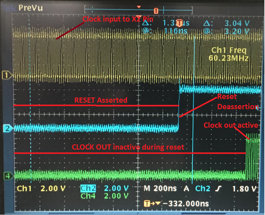
    Below are details on our finding with respect to Clock out, when Reset is asserted.


    EVM / Hardware platform used – C5509A DSK


    EVM Modifications:

    1. Modifications were done to the existing board to add capability to drive clock from external source. DSK by default uses the internal clock.
    2. Applied external clock source to Clock input pin.
    3. 60MHz external clock input was applied.
    4. Reset was asserted and de-asserted using Reset button in the EVM.

    Observations:

    • Attached snapshot captures details on clock out and reset.


    • During Reset assertion No Clock was observed on the clock out pin.
    • Clock out will be active only after releasing the reset (De-asserting reset).

    Conclusion:


    With the above experiment on DSK C5509A, it looks like the clock out is inactive during reset assertion and clock out will become active only after releasing the reset.


    To Note:

    • This is tried only on a single EVM platform (DSK C5509A), so our observations described above is only limited to this EVM/HW platform.
    • Also no experiments were tried on C5503 device, as we do not have a C5503 specific HW platform.

    Hope this helps to conclude.

    Regards

     Vasanth

  • Hi Vasanth,
    Thank you for providing your report to us.
    I will inform this to my customer. If I get more questions from them, please let me confirm them.

    Best regards.
    Kaka