This thread has been locked.

If you have a related question, please click the "Ask a related question" button in the top right corner. The newly created question will be automatically linked to this question.

C6657 DDR3 DQ vs DQS timing

Other Parts Discussed in Thread: CDCM6208

Thank you for all your support.

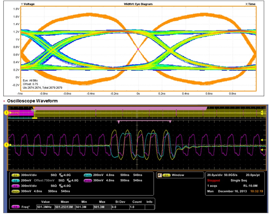
During debugging unstable DDR3 memory access, I found out "unexpected write access timing" as attached. It seems that DQ and DQS timing is shifted by 45 degree, and I believe this should be right in the center. I was wondering if any of you could advise me how to fix this. The configuration is below. I appreciate this.

DSP: TMS320C6657CZH25

memory, Micron: MT41J128M16HA-125

8 banks open for interleaving
RZQ/2
RZQ/2
RZQ/7
CWL = 8
32-bit bus width
CAS = 11
14 row bits
8 bank SDRAM
Use DCE0# for all SDRAM accesses
1024-word page

  • Where were these signals measured? Do you see the same shift if the signal is measured at the vias next to the SOC?

    Regards, Bill

  • Hi Bill

    These signals are measured at the vias right next to the DDR memory pads.

    Thank you

    Matsuno

  • Hi Matsuno,

    If they are measured at the via next to the DDR memory pads than the measurement includes the delay through the traces on the board. Are you trace lengths matched as defined in the DDR3 design requirements? What is the length of each trace and what layers are they routed on?

    Regards, Bill

  • I have the same problem.  The DQS strobes are NOT centered in the data bit window which is causing a marginal hold time condition.   Our system is working with DDR3-1333 but with little timing margin.    I was told that this is NOT programmable in the DSP and that I must have a layout problem.  I do NOT have a layout problem and I have not been given an adequate explanation as to why the device operates this way. 

  • Hi Bill

    Thank you for your support.

    The ones measured, DQS_P0, DQS_N0, and DQ5 have 37.154, 37.148, and 37.010 mm respectively in their length meeting the requirement( <0.25mm). They are all strip line (inner layer) .  Any advice would be appreciated.

    Thank you

    matsuno

  • Hi Matsuno,

    The response to your post may get delayed due to Christmas and New Year Holidays.

    Kindly bear with us.

    Thanks.

  • Hi Matsuno,

    Could you share your DDR3 initialization routine?

  • Hi Aditya

    Thank you for your support.

    Initialization routine is attached(ddr3.c). Basically this is from evaluation board sample code.

    Thank you

    matsuno

  • Hi Matsuno,

    We recently discovered a bug in our C665x DDR3 initialization sequence. Please see the attached GEL file which contains the updated sequence. The updates to our documentation will be rolled into the DDR3 Users guide and Keystone DDR3 initialization app note in the near future.

    Please update your sequence and let us know your observations. Apologize for any inconvenience.

    8863.evmc6657l_ak.gel

  • We reviewed this gel file and implemented all of the changes we found.  It made no difference in the write timing. The data strobe sample point is not centered in the data bit window and as a result the hold time is still marginal.  

  • One question we ask everyone facing DDR3 issues that have no apparent software bugs in their init sequence is: are you following all the requirements listed in the DDR3 design requirements guide? Do you have a spreadsheet with these trace lengths (address, command, control, data group, clock signals) showing you meet the requirements?

  • All layout guidelines were followed.  In particular the data bits and strobes were matched exactly within each byte lane.  You can contact 'Meixner, David' (dmeixner@ti.com) for our history on this problem as he has already asked these questions.   

  • I will check with David.

    • Have you have your initialization sequence reviewed as well?
    • How many boards do you see this issue on and do they all have identical layouts?
    • Are there boards that do not show this issue?
    • Does the problem go away at a lower DDR speed?
  • Hi Matsuno,

    Any update with the new GEL sequence?

  • We have not had our initialization sequence formally reviewed; I will forward this to you.  All boards have the same layout and behave the same way.   We have not done testing at lower speeds.  This issue is not creating a functional problem for us; the product is working reliably at a 667Mhz clock using DDR-1333 speed grade memory.   The concern is that the write data hold time is barely meeting memory specs because the sampling point is shifted 45 degrees (as Matsuno also pointed out) and that variations in process may induce a functional problem in the future.     

  • Init code is attached.

    ddr3_init.docx
  • Hi Aditya

    Thank you for your support.

    I have not had a chance to check the waveform with the new GEL sequence yet, since high-speed scope has not been available until end of this month. I'll let you know as soon as it's ready and I observe it.

    However, it makes "difference" in the behavior with the new GEL in our system. "No memory check error" is observed in my test routine with the new GEL. 

    Thank you

    matsuno

  • Both individuals posting to this thread are concerned about DDR3 write timing.  This is surprising.  DDR3 write timing is the most robust and has the most timing margin.  DDR3 interface integrity problems are almost always read related since the margins are smaller.  I see the waveforms posted but I want to understand why there is an expectation that the write timing is a problem.  Additionally, the related timing between the data strobe DQS/DQS# and data bits DQn is controlled entirely in the silicon IP design and PCB layout.  This is not controllable by leveling adjustment.

    There are numerous forum threads on this topic.  Please refer to http://e2e.ti.com/support/dsp/c6000_multi-core_dsps/f/639/t/245304.aspx as an example.  It lists the steps required to validate a DDR3 layout.  The sequence of steps from that thread is copied below:

    First, you need to lay out the board by following the routing rules stated in the DDR3 Design Requirements for KeyStone Devices at: http://www.ti.com/litv/pdf/sprabi1a.  Most importantly, the length matching rules for the net classes need to be met.  I recommend creation of a spreadsheet to validate that these rules are met.  An example spreadsheet generated from the layout tool is attached here.

    8473.Shn_EVM_DDR3_Rules_1201.xls

    From this table, you can extract the routed lengths for each of the data groups and for the address/command/control/clock fly-by routes from the controller to each of the DRAMs.  This information must be placed into the PHY_CALC spreadsheet.  It and its associated Ap Note are available at: http://www.ti.com/litv/pdf/sprabl2a and http://www.ti.com/litv/zip/sprabl2a.  The PHY_CALC spreadsheet will provide the initialization values needed for your board design.  These links will also provide the REG_CALC spreadsheet which can be used to calculate the remainder of the necessary configuration values.

    If you have done all of this and your design is not functional, please provide the routed length spreadsheet, PHY_CALC and REG_CALC spreadsheets for review.

    Also, please describe your mode of failure and your method for testing the robustness of the memory interface.  If there are failures observed, are they read or write failures?  Repeated reads of the failed location can indicate the mode of failure.

    Tom


  • We are not experiencing any failures.   The problem is our expectation that the DQS/DQS# crossover point (sample point) would be centered in the DQn window to maximize timing margin for setup and hold time.   Instead, the sample point is biased to favor setup time and barely meets hold time.   If this was deliberate in the design of the silicon I would like to understand the reasoning.   - thank you

  • James,

    I was forwarded additional information on the issue that you have been reporting.  We need to review and get back to you.  The sample point is ideally set to the most robust sampling point while accounting for all variations of voltage, silicon, temperature and aging.  This is not necessarily in the middle at a random PVT point for a given chip.  Do you see this on multiple boards?  Do all boards tested contain chips from the same order batch?

    Tom


  • We have made the same measurement on 3 different boards.  The first board used the slower speed grade silicon (TMS320C6657CZH8).   The 2 more recent boards used faster silicon (TMS320C6657CZH) but the DDR3 timing was similar in all cases.  

  • James,

    Can you provide Time Of Flight measurements for these data group nets?  We want the delays caused by the via barrels to also be included.  Can you also provide the stackup and layout images of the DDR3 routing?

    Tom


  • Hi Tom,

    The printed circuit board stack-up, impedances, routing, and lengths are in the attached Word file.   The measurements for each byte lane are "ball to ball" and include vias and fan-outs.

    thanks

    Jim

    IPC board stackup routing.docx
  • Jim,

    When you say the data group nets match length exactly, what does this mean?  Are they all within 1 mil?

    Can you also provide the dielectric thicknesses in the stackup?  Specifically, what are the thicknesses between layers 8, 9, 10 and 11?

    Tom


  • Each data group is matched to the limits of our tool which is 0.00001 inches.  The detailed stack-up and impedance report is attached.  

    impedance and stack up 602224001.pdf
  • James,

    You indicate that you have this interface functional.  Do you have a functional GEL with the configuration parameters?  What speed DDR reference clock and DDR clock are you using?  Are you using Partial Automatic or Full automatic leveling?

    Tom


  • Hi Tom,

    Our init code was posted on Jan 16.   We are fully functional with a DDR3 clock of 667Mhz on sixty-five boards.   The reference clock is 66.67Mhz generated by the TI CDCM6208 clock chip.   The purpose of this inquiry is to simply understand why the DQS edge is not positioned closer to the center of the data bit window to give more hold time margin for write data.   This is the expected norm based on another DDR3 design we have working on the same board for our host cpu.   

    Jim

  • Jim,

    OK, looking back in to the code I see that you are using the proper register initialization for Partial Automatic leveling that was released a few weeks back.  I wanted to be sure that this condition was not connected to programming the registers on this device incorrectly.

    Tom


  • Hi Tom,

    I posted two scope shots that were saved using the TEK/DSA70804C scope and TEK/P7380A differential probes.  

    thanks

    Jim 

    scope shots.docx
  • Jim,

    I want to let you know that we have not forgotten about this issue.  We have busy with other activities.  We are coordinating the right resources to address this in the coming weeks.

    Tom


  • Hi Tom,

    Could you please let me know whether this issue has been solved or not?
    Because I have the same problem now.

    Regards,
    j-breeze

  • Hi,

    I need to get any workarounds for this issue until next Monday morning Japan time.
    So, doesn't someone know that?

    Thanks in advance for your cooperation.

    Regards,
    j-breeze

  • We still have this issue but it has NOT caused any functional problems after building a few hundred boards.

  • Hi james,

    Thank you for your information. I'm not sure, but I think there are any reliability problems.
    I'll check out the detailed write leveling spec.

    Regards,
    j-breeze

  • A solution is available for this problem.  The team conducting tests on this issue were able to observe a similar DQS-DQ shift as observed.  We reviewed this observed behavior with the Silicon Design Team.  With their help we identified a previously undocumented register that controls this offset.  It appears that the default value in this register in C665x devices does not result in an optimum offset between DQS to DQ for writes.  Once the proper value 0x40 is loaded into the data_reg_phy_dq_offset in bits 24:18 of the DDR3_CONFIG_REG_1 at offset 0x408 as part of the DDR3 initialization process, the proper DQS-DQ offset is obtained.  Please see the GEL excerpt below which shows the additions needed to the C665x DDR3 configuration process to correct for this issue.  Please confirm that this resolves the DQ-DQS issue observed.

    We will be updating the online documentation in the coming weeks to contain this corrected procedure.

    See below code snippet of C665x GEL – changes highlighted in bold text:


    ... 

    #define DDR3_CONFIG_REG_1    (*(unsigned int*)(CHIP_LEVEL_REG + 0x0408))


    ddr3_setup_auto_lvl_1333()

    {

        int i,TEMP,startlo, stoplo,starthi, stophi;

        KICK0 = KICK0_UNLOCK;

        KICK1 = KICK1_UNLOCK;


        /* Wait for PLL to lock = min 500 ref clock cycles.

           With refclk = 100MHz, = 5000 ns = 5us */

        Delay_milli_seconds(1);


        /***************** 3.2 DDR3 PLL Configuration ************/

        /* Done before */


        /**************** 3.0 Leveling Register Configuration ********************/

        /* Using partial automatic leveling due to errata */


        /**************** 3.3 Leveling register configuration ********************/

        DDR3_CONFIG_REG_0 &= ~(0x007FE000);  // clear ctrl_slave_ratio field

        DDR3_CONFIG_REG_0 |= 0x00200000;     // set ctrl_slave_ratio to 0x100

        DDR3_CONFIG_REG_12 |= 0x08000000;    // Set invert_clkout = 1

        DDR3_CONFIG_REG_0 |= 0xF;            // set dll_lock_diff to 15


        //From 4.2.1 Executing Partial Automatic Leveling -- Start


           DDR3_CONFIG_REG_52 |= 0x00000200;

           DDR3_CONFIG_REG_53 |= 0x00000200;

           DDR3_CONFIG_REG_54 |= 0x00000200;

           DDR3_CONFIG_REG_55 |= 0x00000200;

           DDR3_CONFIG_REG_60 |= 0x00000200;


        //From 4.2.1 Executing Partial Automatic Leveling -- End

        //Values with invertclkout = 1 and v10 of PHY_CALC

        /**************** 3.3 Partial Automatic Leveling ********************/


           //Correct DQS-DQ timing offset

           DDR3_CONFIG_REG_1 = 0x01000000;


           DATA0_WRLVL_INIT_RATIO = 0x6C;

           DATA1_WRLVL_INIT_RATIO = 0x6C;

           DATA2_WRLVL_INIT_RATIO = 0x7A;

           DATA3_WRLVL_INIT_RATIO = 0x73;

           DATA8_WRLVL_INIT_RATIO = 0x5C;


           DATA0_GTLVL_INIT_RATIO = 0xB0;

           DATA1_GTLVL_INIT_RATIO = 0xB0;

           DATA2_GTLVL_INIT_RATIO = 0xBD;

           DATA3_GTLVL_INIT_RATIO = 0xC3;

           DATA8_GTLVL_INIT_RATIO = 0xA4;


        //Do a PHY reset. Toggle DDR_PHY_CTRL_1 bit 15 0->1->0

        DDR_DDRPHYC &= ~(0x00008000);

        DDR_DDRPHYC |= (0x00008000);

        DDR_DDRPHYC &= ~(0x00008000);


    Tom

  • We implemented this change and DO see improved margins in the write timing.  Thank you for your attention to this matter!

  • The revised K1 DDR3 Init Guide and the revised K1 DDR3 Controller User Guide containing this new guidance have been released to the web. The revised EVM GEL file in the EMU Pack and a Usage Note in the Errata document are in the works.
    Tom