This thread has been locked.

If you have a related question, please click the "Ask a related question" button in the top right corner. The newly created question will be automatically linked to this question.

CDCE62005 generates clock for TMS320C6678

Other Parts Discussed in Thread: CDCE62005

Hello, all,

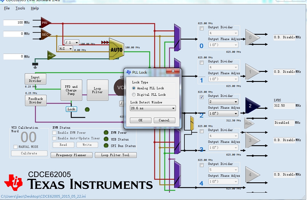
I designed a board based on EVM6678, now I face a problem, the SGMII can't work well. I have asked for many suggestions, someone said it's because the instability of clock. I used the software to config the register, but the pll is still unlocked, and I don't know how to make the clock in a better condition. Someone can give me some advice? Thank you very much!!!

  • Hi,

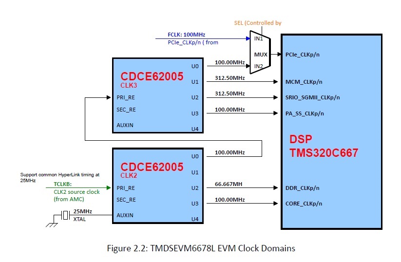
    Have you using the same EVM6678 clock design on your custom board? Input clock is 25Mhz.

    Thanks,

  • Yes, I used the same circuit with EVM board, but the EVM can lock the pll properly, and my board can not.
  • Have you run the same example on both targets?
    Have you probe/verify the SGMII reference clock on EVM and your custom board? it does not show the same frequency.

    Thanks,
  • Thank for your attention!!! As the figure above, I use the TI EVM software to get the register config, and save it as the *.ini file, in this file, we can get the 9 registers value.

    And I burn the config value by FPGA, the code module is:


    // =================================================================================================
    // Project Name   :
    // File Name      : clk_cfg.v
    // Module         : CLK_CFG
    // Level          : 1
    // Upper Module   :
    // Down Module    :
    // Function       : 时钟管理芯片配置
    // Type           : RTL
    // -------------------------------------------------------------------------------------------------
    // Update History :
    // -------------------------------------------------------------------------------------------------
    // Rev.Level  Date        Coded by       Contents
    // 0.0.1      2008/08/05                   Create new
    //
    // -------------------------------------------------------------------------------------------------
    // Update Details :
    // -------------------------------------------------------------------------------------------------
    // Date         Contents Detail
    //
    //
    // =================================================================================================
    // End Revision
    // =================================================================================================


     //---- note 1
     /**************************************************************************\
      SPI_MISO : LVCMOS input
      SPI_MOSI : LVCMOS output
      SPI_CLK  : LVCMOS output
      SPI_LE  : LVCMOS output
     \**************************************************************************/

     //---- note 2
     /**************************************************************************\
      REF_SEL  : 1: PRI  0: SEC     --> REF_SEL  = 1'b1
      CLK_PD  : active low for the device reset  --> CLK_PD  = 1'b1
      TEST_MODEL : must be tied high     --> MODE_SEL = 1'b1
     \**************************************************************************/

     //---- note 2
     /**************************************************************************\
              ___________
             | OUTPUT  |         ___________
     PRI_IN(64M LVDS) ---------|  MUX  |--------|____/1_____|--------> 64M LVPEAL
             |_ CONTROL__|   |
                   |    ___________
                   |---|____/2_____|--------> 32M LVPEAL
                   |
                   |    ___________
                   |---|____/2_____|--------> 32M LVPEAL
                   |
                   |    ___________
                   |---|____/2_____|--------> 32M LVPEAL

     \**************************************************************************/

    `timescale 1ns/1ps

    module clk_cfg
     (
     //----<< global signal  >>------
     CLK33M  ,      //(I)   33Mhz input
     nRESET  ,

     //----<< CDCE62005 IF  >>------
     REF_SEL  ,
     CLK_PD  ,
     TEST_MODEL ,

     SPI_CLK  ,      //(O)   config clock
     SPI_MOSI ,      //(O)   FPGA --> CDCE62005 (config data)
     SPI_MISO ,      //(I)   CDCE62005 --> FPGA (regest data)
     SPI_LE        //(O)   SPI enable

     );

     //------------------------------------------------------
     //---- port define
     //------------------------------------------------------

     input   CLK33M  ;
     input   nRESET  ;

     output   REF_SEL  ;
     output   CLK_PD  ;
     output   TEST_MODEL ;

     output   SPI_CLK  ;
     output   SPI_MOSI ;
     input   SPI_MISO ;
     output   SPI_LE  ;

     //------------------------------------------------------
     //---- signal define
     //------------------------------------------------------

     //---- I/O FF
     reg    R_SPI_CLK ;
     reg    R_SPI_MOSI ;
     reg    R_SPI_LE ;

     //---- CLK&RESET
     reg  [ 2:0] R_ClkCnt ;
     wire   S_SPI_CLK ;
     wire   S_SPI_CLK_n ;

     //---- parameter

      //---- SPI register         //  2222 2222 1111 1111 11
                                  //  7654 3210 9876 5432 1098 7654 3210
     parameter     REG0  = 32'hE9060320 ,
           REG1  = 32'hE90E0301 ,
                  REG2  = 32'hE90E0302 ,
           REG3  = 32'hE90E0303 ,
           REG4  = 32'hE90E0314 ,
           REG5  = 32'h298C0305 ,
           REG6  = 32'h84D219B6 ,
           REG7  = 32'hD50037B7 ,
                             StaCtrl  = 32'h20005FF8 ,
    //     READ1  = 32'b0000_0000_0000_0000_0000_0000_0000_1110 , //read cmd
    //     READ2  = 32'b0000_0000_0000_0000_0000_0000_0001_1110 , //read cmd
    //     READ3  = 32'b0000_0000_0000_0000_0000_0000_0010_1110 , //read cmd
    //     READ4  = 32'b0000_0000_0000_0000_0000_0000_0011_1110 , //read cmd
    //     READ5  = 32'b0000_0000_0000_0000_0000_0000_0100_1110 , //read cmd
    //     READ6  = 32'b0000_0000_0000_0000_0000_0000_0101_1110 , //read cmd
    //     READ7  = 32'b0000_0000_0000_0000_0000_0000_0110_1110 , //read cmd
    //     READ8  = 32'b0000_0000_0000_0000_0000_0000_0111_1110 , //read cmd
    //                    READ9  = 32'b0000_0000_0000_0000_0000_0000_1000_1110 , //read cmd

         unlock  = 32'b0000_0000_0000_0000_0000_0000_0001_1111 ; //ram --> e2prom unlock

     //---- internal signal

     reg  [ 2:0] R_LE_CNT ;
     reg    R_LE  ;
     reg  [31:0] R_SFT  ;
     reg  [ 4:0] R_SFTCNT ;
    // wire [31:0] S_SFT  ;
     reg    R_SFT_LD ;
     reg  [ 4:0] R_dcnt  ;
     reg  [ 9:0] R_PWRON_WAIT;

     reg    R_PWRON_RDY ;


     //--------------------------------------------------------------------------
     //---- RTL BODY
     //--------------------------------------------------------------------------

     //---- POWER ON wait
        always @ (posedge CLK33M or negedge nRESET) begin
      if(~nRESET) begin
       R_PWRON_WAIT <= 10'b0;
      end else begin
             R_PWRON_WAIT <= R_PWRON_WAIT + 1'b1;
      end
     end

        always @ (posedge CLK33M or negedge nRESET) begin
      if(~nRESET) begin
       R_PWRON_RDY <= 1'b0;
      end else begin
       if (R_PWRON_WAIT == {10{1'b1}}) begin
         R_PWRON_RDY <= 1'b1;
       end
      end
     end


        // TEST
    // reg         R_PWRON_RDY_DLY ;
    // wire        S_PWRON_RDY_UP  ;
    // reg         R_PWRON_RDY_UP  ;
    //
    // always @ (posedge CLK33M or negedge nRESET) begin
    //  if(~nRESET) begin
    //   R_PWRON_RDY_DLY <= 1'b0;
    //  end else begin
    //   R_PWRON_RDY_DLY <= R_PWRON_RDY;
    //  end
    // end
    //
    // assign S_PWRON_RDY_UP = R_PWRON_RDY & (~R_PWRON_RDY_DLY) ;
    //
    //    always @ (posedge CLK33M or negedge nRESET) begin
    //  if(~nRESET) begin
    //   R_PWRON_RDY_UP <= 1'b0;
    //  end else begin
    //   R_PWRON_RDY_UP <= S_PWRON_RDY_UP;
    //  end
    // end

        //

     //---- clk count
     always @ (posedge CLK33M or negedge nRESET) begin
      if(~nRESET) begin
       R_ClkCnt <= 3'b0;
      end else begin
       if (R_PWRON_RDY) begin
        R_ClkCnt <= R_ClkCnt + 1'b1;
       end
      end
     end

     assign S_SPI_CLK = R_ClkCnt[2]  ;
     assign S_SPI_CLK_n = (R_ClkCnt == 3'b111) ;

     //---- LE control cnt
     always @ (posedge CLK33M or negedge nRESET) begin
      if(~nRESET) begin
       R_LE_CNT <= 3'b0;
      end else if (S_SPI_CLK_n) begin
       if (R_LE) begin
        R_LE_CNT <= R_LE_CNT + 1'b1;
       end else begin
        R_LE_CNT <= 3'b0;
       end
      end
     end

     //---- LE
     always @ (posedge CLK33M or negedge nRESET) begin
      if(~nRESET) begin
       R_LE <= 1'b1;
      end else if (S_SPI_CLK_n) begin
    //   if ((R_LE_CNT == 3'b111) && (R_dcnt != 5'b10100)) begin
       if ((R_LE_CNT == 3'b111) && (R_dcnt != 5'b01010)) begin
        R_LE <= 1'b0;
       end else if (R_SFTCNT == 5'b11111) begin
        R_LE <= 1'b1;
       end
      end
     end

     //---- SFT count
     always @ (posedge CLK33M or negedge nRESET) begin
      if(~nRESET) begin
       R_SFTCNT <= 5'b11111;
      end else if (S_SPI_CLK_n) begin
       if (R_LE) begin
        R_SFTCNT <= 5'b0;
       end else begin
        R_SFTCNT <= R_SFTCNT + 1'b1;
       end
      end
     end

     //---- R_SFT_LD
     always @ (posedge CLK33M or negedge nRESET) begin
      if(~nRESET) begin
       R_SFT_LD <= 1'b0;
      end else begin
       if (S_SPI_CLK_n && (R_SFTCNT == 5'b11111)) begin
        R_SFT_LD <= 1'b1;
       end else begin
        R_SFT_LD <= 1'b0;
       end
      end
     end

     //---- R_dcnt write ram number
     always @ (posedge CLK33M or negedge nRESET) begin
      if(~nRESET) begin
       R_dcnt <= 5'b0;
      end else begin
       if (R_SFT_LD) begin
        R_dcnt <= R_dcnt + 1'b1;
       end
      end
     end

     //---- S_SFT
    // assign S_SFT = (R_dcnt == 5'b00000) ? REG0  :
    //      (R_dcnt == 5'b00001) ? REG1  :
    //      (R_dcnt == 5'b00010) ? REG2  :
    //      (R_dcnt == 5'b00011) ? REG3  :
    //      (R_dcnt == 5'b00100) ? REG4  :
    //      (R_dcnt == 5'b00101) ? REG5  :
    //      (R_dcnt == 5'b00110) ? REG6  :
    //      (R_dcnt == 5'b00111) ? REG7  :
    ////                        (R_dcnt == 5'b01000) ? READ1  :
    ////                        (R_dcnt == 5'b01001) ? READ2  :
    ////                        (R_dcnt == 5'b01010) ? READ3  :
    ////                        (R_dcnt == 5'b01011) ? READ4  :
    ////                        (R_dcnt == 5'b01100) ? READ5  :
    ////                        (R_dcnt == 5'b01101) ? READ6  :
    ////                        (R_dcnt == 5'b01110) ? READ7  :
    ////                        (R_dcnt == 5'b01111) ? READ8  :
    ////                        (R_dcnt == 5'b10000) ? READ9  :
    ////                        (R_dcnt == 5'b10001) ? StaCtrl  : unlock ;
    //                        (R_dcnt == 5'b01000) ? StaCtrl  : unlock ;

     reg  [31:0] R_SEL_DATA1 ;
     reg  [31:0] R_SEL_DATA2 ;
     reg  [31:0] R_SEL_DATA3 ;
     reg  [31:0] R_SEL_DATA4 ;

     wire   S_SEL1 ;
     wire   S_SEL2 ;
     wire   S_SEL3 ;
     wire   S_SEL4 ;
     wire   S_SEL5 ;

     wire   S_SEL6 ;
     wire   S_SEL7 ;
     wire   S_SEL8 ;


     assign S_SEL1 = (R_dcnt[4:1] == 4'B0000) ;
     assign S_SEL2 = (R_dcnt[4:1] == 4'B0001) ;
     assign S_SEL3 = (R_dcnt[4:1] == 4'B0010) ;
     assign S_SEL4 = (R_dcnt[4:1] == 4'B0011) ;

     assign S_SEL5 = (R_dcnt[4:2] == 3'B000) ;
     assign S_SEL6 = (R_dcnt[4:2] == 3'B001) ;

     assign S_SEL7 = (R_dcnt[4:3] == 4'B00) ;
     assign S_SEL8 = (R_dcnt[4:3] == 4'B01) ;


     reg  [31:0] R_SEL_DATA5 ;
     reg  [31:0] R_SEL_DATA6 ;

     reg  [31:0] R_SEL_DATA7 ;

     reg  [31:0] R_SEL_DATA8 ;

     reg  [31:0] R_SEL_DATA9 ;

     always @ (posedge CLK33M or negedge nRESET) begin
      if(~nRESET) begin
       R_SEL_DATA1 <= 32'b0;
      end else begin
       case (R_dcnt)
        5'b00000 : R_SEL_DATA1 <= REG0;
                    5'b00001 : R_SEL_DATA1 <= REG1;
       endcase
      end
     end

     always @ (posedge CLK33M or negedge nRESET) begin
      if(~nRESET) begin
       R_SEL_DATA2 <= 32'b0;
      end else begin
       case (R_dcnt)
        5'b00010 : R_SEL_DATA2 <= REG2;
                    5'b00011 : R_SEL_DATA2 <= REG3;
       endcase
      end
     end

     always @ (posedge CLK33M or negedge nRESET) begin
      if(~nRESET) begin
       R_SEL_DATA3 <= 32'b0;
      end else begin
       case (R_dcnt)
        5'b00100 : R_SEL_DATA3 <= REG4;
                    5'b00101 : R_SEL_DATA3 <= REG5;
       endcase
      end
     end

     always @ (posedge CLK33M or negedge nRESET) begin
      if(~nRESET) begin
       R_SEL_DATA4 <= 32'b0;
      end else begin
       case (R_dcnt)
        5'b00110 : R_SEL_DATA4 <= REG6;
                    5'b00111 : R_SEL_DATA4 <= REG7;
       endcase
      end
     end

     always @ (posedge CLK33M or negedge nRESET) begin
      if(~nRESET) begin
       R_SEL_DATA9 <= 32'b0;
      end else begin
       case (R_dcnt)
        5'b01000 : R_SEL_DATA9 <= StaCtrl;
                    5'b01001 : R_SEL_DATA9 <= unlock;
       endcase
      end
     end

     always @ (posedge CLK33M or negedge nRESET) begin
      if(~nRESET) begin
       R_SEL_DATA5 <= 32'b0;
      end else begin
       if (S_SEL1) begin
        R_SEL_DATA5 <= R_SEL_DATA1;
       end else if (S_SEL2) begin
        R_SEL_DATA5 <= R_SEL_DATA2;
       end
      end
     end

     always @ (posedge CLK33M or negedge nRESET) begin
      if(~nRESET) begin
       R_SEL_DATA6 <= 32'b0;
      end else begin
       if (S_SEL3) begin
        R_SEL_DATA6 <= R_SEL_DATA3;
       end else if (S_SEL4) begin
        R_SEL_DATA6 <= R_SEL_DATA4;
       end
      end
     end

     always @ (posedge CLK33M or negedge nRESET) begin
      if(~nRESET) begin
       R_SEL_DATA7 <= 32'b0;
      end else begin
       if (S_SEL5) begin
        R_SEL_DATA7 <= R_SEL_DATA5;
       end else if (S_SEL6) begin
        R_SEL_DATA7 <= R_SEL_DATA6;
       end
      end
     end

     always @ (posedge CLK33M or negedge nRESET) begin
      if(~nRESET) begin
       R_SEL_DATA8 <= 32'b0;
      end else begin
       if (S_SEL7) begin
        R_SEL_DATA8 <= R_SEL_DATA7;
       end else if (S_SEL8) begin
        R_SEL_DATA8 <= R_SEL_DATA9;
       end
      end
     end

     reg [31:0] R_SFT_D1;

     always @ (posedge CLK33M or negedge nRESET) begin
      if(~nRESET) begin
       R_SFT_D1 <= 32'b0;
      end else begin
       R_SFT_D1 <= R_SEL_DATA8;
      end
     end

     //---- R_SFT
     always @ (posedge CLK33M or negedge nRESET) begin
      if(~nRESET) begin
       R_SFT <= 32'b0;
      end else begin
       if (R_SFT_LD) begin
    //    R_SFT <= S_SFT ;
        R_SFT <= R_SFT_D1 ;
       end else if (S_SPI_CLK_n & ~R_LE) begin
        R_SFT <= {R_SFT[0],R_SFT[31:1]} ;
       end
      end
     end

     //---- ioff
     always @ (posedge CLK33M or negedge nRESET) begin
      if(~nRESET) begin
       R_SPI_CLK <= 1'b0;
       R_SPI_MOSI <= 1'b0;
       R_SPI_LE <= 1'b0;
      end else begin
       R_SPI_CLK <= S_SPI_CLK ;
       R_SPI_MOSI <= R_SFT[0]  ;
       R_SPI_LE <= R_LE   ;
      end
     end

     assign SPI_CLK  = R_SPI_CLK ;
     assign SPI_MOSI = R_SPI_MOSI ;
     assign SPI_LE     = R_SPI_LE ;

     assign REF_SEL  = 1'b1  ;
     assign CLK_PD  = 1'b1  ;
     assign TEST_MODEL = 1'b1  ;


    endmodule

    And I used to burn it to EVM board, it worked. But on my board, it cannot work.

  • I am sorry, the figures are:

  • I am sorry, the figures are:

  • Hello Zhuang,

    Did you probe the SGMII reference clock ? Are you getting the proper frequency ?

    If not, as you said the problem would be on the CDCE62005 PLL lock.

    Since this forum deals with the queries related to the DSP device, i would request you to post this query in below forum.

    https://e2e.ti.com/support/clocks/

    Regards,
    Senthil

  • Hello, I have probed the EVM board and my board, and I found that the SGMIICLK had nothing different. Is the SGMII interface so sensitive to clock? If the clock is not in a best condition, what can I do to make the SGMII work normally? Is there any metherd? Thank you!!! 

  • Hello Zhuang,

    What is the clock frequency you are using for SGMII reference clock ?

    Could you please elaborate the issue you are facing with SGMII ?

    Have you tried internal loopback test ?

    Is there any difference in hardware in your custom board with respect to EVM ?

    Regards,
    Senthil