This thread has been locked.

If you have a related question, please click the "Ask a related question" button in the top right corner. The newly created question will be automatically linked to this question.

[C6655, uPP] uPP does not work in receive mode

Hello,

My customer is developing their system with C6655 and using its uPP in receive mode (16bit).
They are getting stuck with very strange behavior...
We need to clarify uPP behavior. uPP is very very important transport in their application.
Hope you could reply soon.

So, here is the problem.

C6655 does not receive incoming data correctly. 
Their system works as below. Please note this is just a test application to verify uPP transport.

1. C6655 setups uPP DMA to receive a single window, which a window is constructed from a single 64byte line.
    After configuring uPP DMA, C6655 signals uPP host via GPIO. When incoming data reaches to 64bytes, an interrupt is
    generated and C6655 checks the contents of input buffer whether it is expected data or not. And lastly,
    C6655 setups uPP DMA for next 64byte reception, and then signals to uPP host via GPIO again.
    The system works like this. Please note, cache is being disabled in system.

2. Now uPP host side.
    After getting the GPIO notification, uPP host understands C6655 has been completed to configure
    uPP DMA to receive 64byte chuck and starts transfer. 
    The waveform looks like this at the beginning of each 64byte chunk.
    As you see, there is no waveform for data lines, but please assume the data lines are always driven
    at each START/ENABLE activation and all signals are being latched by CLOCK on rising edge.
    Also, please note my customer had been verified that there was no WAIT signal activation during the transfer.
    - Yellow : CLOCK
    - Green : START
    - Magenta : ENABLE
    - Blue : WAIT

3. It seems the uPP host is sending each 64byte chunks perfectly.
    We don't find any errors in software logic in uPP host side and any AC timing violations in waveform.
    However, C6655 misses some 64byte lines !! Here is erroneous scenario:

    uPP Host                                   C6655
    <1st 64byte chunk>  ------------- No interrupt happens. No valid data in receive buffer. 
    <2nd 64byte chunk> ------------- No interrupt happens. No valid data in receive buffer. 
    <3rd 64byte chunk> -------------- Transfer completion interrupt happens. <2nd 64byte chunk> is received, rather than <3rd 64byte chunk>
    <4th 64byte chunk>------------- No interrupt happens. No valid data in receive buffer. 

    <5th 64byte chunk>------------- No interrupt happens. No valid data in receive buffer. 
    <6th 64byte chunk>-------------- Transfer completion interrupt happens. <5th 64byte chunk> is received, rather than <6th 64byte chunk>

   1st, 3rd, 4th, and 6th frames are completely missed. Also, 2nd and 5th frames are received and their contents is expected,
   but these are "delayed" to 
the next time frame.

Well, that is our current situation, but we found a workaround -- this looks curious workaround however.
When uPP host intentionally inserts dummy clocks at the end and at the beginning of
each chunk, all chunks are transferred correctly! The workaround looks like this :

    uPP Host                                                                                           C6655
   <3 dummy clocks ,1st 64byte chunk, 2 dummy clocks>  -------------  <1st 64byte chunk> received with correct data

   <3 dummy clocks ,2nd 64byte chunk, 2 dummy clocks>  ------------- <2nd 64byte chunk> received with correct data
   <3 dummy clocks ,3rd 64byte chunk, 2 dummy clocks>  -------------  <3rd 64byte chunk> received with correct data
   <3 dummy clocks ,4th 64byte chunk, 2 dummy clocks>  -------------  <4th 64byte chunk> received with correct data
   <3 dummy clocks ,5th 64byte chunk, 2 dummy clocks>  -------------  <5th 64byte chunk> received with correct data
   <3 dummy clocks, 6th 64byte chunk, 2 dummy clocks>  -------------  <6th 64byte chunk> received with correct data

Please let me know your suspicions for the root cause.
I see may posts about uPP transfer problem, but I could not find any validated answers...

Best Regards,
Kawada

  • Additional information:

    Instead of "dummy clocks", I suggested the customer to insert "some software delay" in uPP host to cover the time
    for "dummy clocks" at the beginning/end of the chunk.
    However, the problem is still there. Actual additional dummy clocks I mentioned in the previous post seems to be required to fix the problem.

    Best Regards,
    Kawada

  • Hello Naoki,

    We are working on this issue. We will get back to you shortly.

    Regards,
    Senthil
  • Hi,

    How about the clock speed ?

    Try to reduce the clock speed and see the behavior.

    Any interrupt status registers got set for missing interrupts  ?

    What is the purpose of GPIO here ?

    1. C6655 setups uPP DMA to receive a single window, which a window is constructed from a single 64byte line.

       After configuring uPP DMA, C6655 signals uPP host via GPIO. When incoming data reaches to 64bytes, an interrupt is

       generated and C6655 checks the contents of input buffer whether it is expected data or not. And lastly,

       C6655 setups uPP DMA for next 64byte reception, and then signals to uPP host via GPIO again.

       The system works like this. Please note, cache is being disabled in system.

    Could you comment out the "data checking" code part and just receive it.

  • Hi Titus S.

    As for clock speed, I'll ask the customer, but I think this would not help.
    The clock speed is in range of datasheet spec.
    And user can receive data when inserting dummy clocks (workaround) with same clock rate.

    And GPIO signaling from C6655 to uPP Host is "ready" signal. GPIO will be triggered (C6655 to uPP Host) after uPP DMA has been configured to accept new data.

    As for the status register, they could not see any errors for missing transfers.

    The checking code works only for the data received from uPP host.
    The problem is, when uPP host sends some frames, uPP sometimes misses the incoming frame completely. No interrupt (related to transfer complete, or errors) happens for the missed frames. C6655 uPP looks ignoring the incoming frame. So, removing checking code will not help.

    Best Regards,
    Kawada
  • Hi Titus S.

    I talked with the customer and asked to slow down the clock to see if what can happen.
    They have tried slow clocks before and the problem seemed to be there, but let us re-confirm again. I'll update you later.
    In the meanwhile, i would like you to consider about the other suspicions.

    Thank you in advance for your help.
    Best Regards,
    Kawada

  • My customer tried to slow down the clock to ~10Mhz, but the problem is still there -- the phenomenon is exactly same with the above report.
    One thing to update you. When they tried to use bigger frame size such like 16Kbytes, the required number of dummy clocks changed also. In case of 16Kbytes per frame, now 6 clocks (not 3, but 6 clocks at the beginning of frame) seems to be required for the correct behavior.

    So what is your findings ?

    Best Regards,
    Kawada

  • Hi Kawada,
    Sorry for the delay in response.
    What is the device has been used for uPP host ?
    FPGA or any DSP/ARM ?
    What type of clock source used at host side since you are inserting dummy clocks.

    We have asked our hw experts also to look into this issue.

  • Hello Titus S.,

    Thanks for your reply.
    uPP host is a generic micro controller (Not Ti device). It has a generic parallel port for external device such like async memory and my customer is using this as a uPP transport with some external logic. As for clock signal, it seems it is being created by its "write enable pin". So, from uC view point, changing the number of dummy clocks means changing the number of "write to the parallel port".

    Best Regards,
    Kawada
  • Kawada,

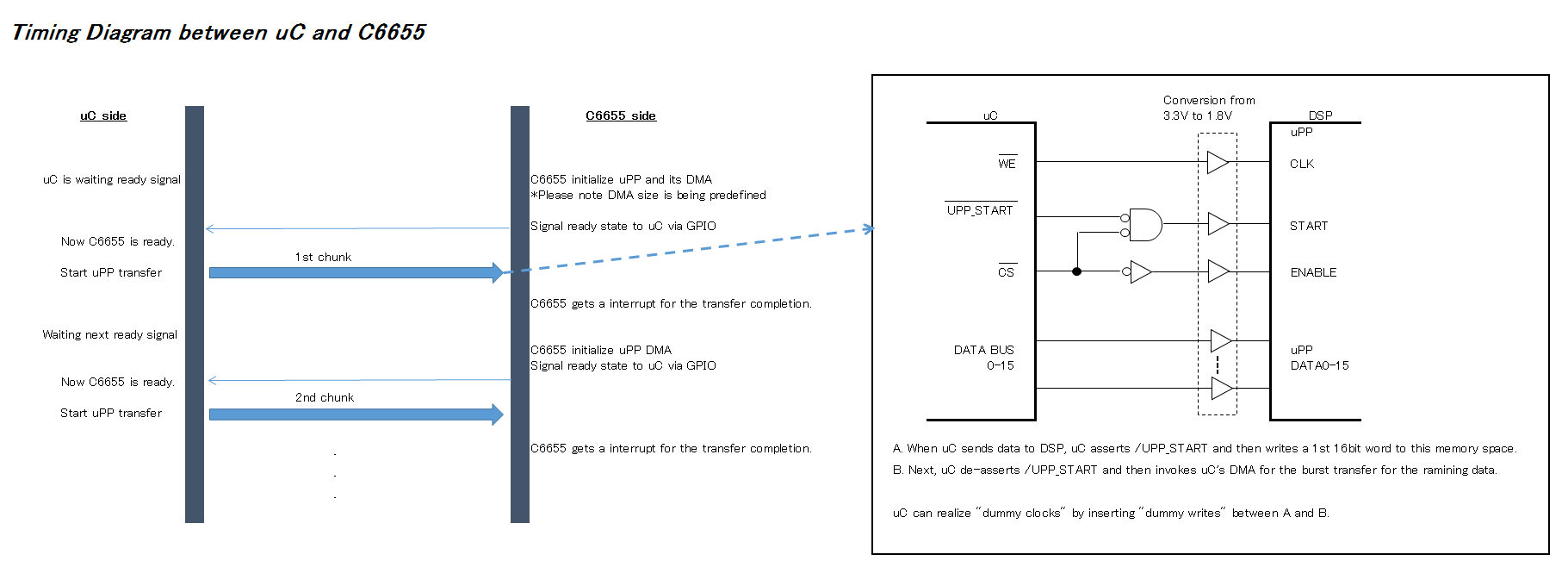
    This appears to be a synchronization problem.  That is probably why it works for a while and then misses a block.  Please put together a block diagram of the implementation showing how the timing is sourced for the transfers.  You state that the UC is using a standard ASYNC bus.  The UC is the timing master of this ASYNC interface.  How is the UPP on C6655 implemented?  What is the source timing for its reads and writes?  What logic lies between?  How are the data transfers arbitrated?  A protocol timing diagram may be useful to see how the 2 sides are cooperating.

    Tom

  • Hello Tom,

    Thank you for your response.
    I'm asking the same to the customer. I'll update you next week.

    Best Regards,
    Kawada
  • Hello Tom,

    Here is timing diagram. Do you have any comments on this ?

    In the meanwhile, I'm asking the customer to insert "software delay" before signaling GPIO to get the time margin for uPP DMA setup.
    uPP might not be actually "ready" state to accept incoming data because of something uPP HW setup time restriction or something SW inconsistence.

    Best Regards,
    Naoki

  • Hello,

    My customer added the software delay which I mentioned in the previous post. They have inserted 900ms (huge) delay before signaling GPIO to uPP Host, but the problem was still there.

    Best Regards,
    Naoki
  • Naoki-san,

    We still need more information to help diagnose the problem.  Perhaps a logic analyzer capture showing all of the signals with enough zoom to see the actual timing and sequence of events.  Actually, we may need to see multiple.  The first needs to show the beginning of the transfer.  The second needs to show the steady-state transfer when it is working.  The third needs to show the transfer that fails.

    Tom

  • Naoki-san,

    Please be sure to show all of the signals including the GPIO status signals.  Also please show a zoom of the stall between 64-byte chunks.  You mention that adding dummy clocks makes it work so we would need to see an LA picture of that as well.

    Tom

  • Hello Tom,

    Can you check the attached waveforms ?

    Best Regards,
    Naoki Kawada

    upp waveforms .xlsx

  • Naoki-san,

    The customer implementation is discontinuous.  They are trying to use the UPP as a slave asynchronous memory interface.  The UPP is designed to transport synchronous streams of data.  Solutions like their work-around of adding dummy clocks may be the only means to make this work.  However, it may still might not be robust.  Please refer to Figure 2-4 and 2-5 in the UPP UG SPRUHG9.  You can see that the clock is continuous and that the when in receive mode, the ENABLE signal qualifies the DATA as being valid.  You can also see in the transmit mode, the WAIT input must be pipelined one clock before the TX data halts.

    Tom

  • What is the clock polarity? Is the CLKINVx bit low indicating all sampling is on the rising edge of clock?
  • Naoki-san,

    Similar to the need for dummy clocks to pre-load the synchronous state machine to make the WAIT signal go inactive, I believe the dummy clocks at the end of the burst are needed to initiate the DMA.  Unless additional logic is added to make this a continuous, streaming clock interface, I believe the only solution is addition of dummy clocks both before and after each 64-byte chunk of data.  Does the customer achieve robust operation with these added?

    Tom

  • Naoki-san,
    In addition to the need for a continuous clock, as Tom described above, it is also a requirement that the WAIT signal be included in the UPP logic as stated in Table 2-5. The WAIT signal is generated by the C6655 and can go high to pause the receive transfer. If the WAIT signal is set high by the receiver, all data transfers will be ignored until the WAIT is set low. The transmit side is responsible for monitoring the WAIT and pausing the data transfer if the WAIT is set high. Based on the results observed, it also appears that the WAIT needs some input clocks to cycle through its state machine. In a system with a continuous clock, this will always occur. In the customers implementation, they might need to perform dummy writes until the WAIT is set low.
    Regards,
    Bill
  • Hello Tom and Bill,

    Thank you very much for your answers.

    We need to clarify the behavior of WAIT signal again.
    I have asked WAIT pin behavior but the answer does not much to your answers:
    ==================================================================
    Mukul stated --  I have confirmed from design that the WAIT signal only asserts on emulation halts and clkstop ( on chip power sleep controller gating of uPP module clocks etc). It does not get asserted on state on internal FIFO / data availability etc. 

    https://e2e.ti.com/support/dsp/c6000_multi-core_dsps/f/639/t/389280

    ==================================================================

    According to your answers, WAIT pin goes active if the clocks are not fed continuously before START signal. And feeding some clocks (in our case, dummy clocks before and after the transfers) makes uPP awake its function. So, how many clocks are required ? As I mentioned before, the number of dummy clocks looks different depending on the transfer size. And what is the purpose of the former dummy clock ? And what about latter ?

    You stated uPP is designed for sync use case, but I can't find the documentation related to this. And there is no max requirements for AC timings of uPP signals. This means uPP could be applicable to async use case, right ? My customer's use case would verify that uPP could be also applicable to async use case if you could clarify the above requirements. Async memory interface is very generic, so we may be able to have opportunities to promote C665x/uPP to other users.

    Best Regards,
    Naoki Kawada 

  • Naoki-san,
    The uPP IP was designed for a continuous clock stream. All the timing diagrams provided for the part clearly show a continuous clock and the transmit clock can only be configured by setting a divider. There is no provision for asynchronous operation on the transmit side.
    The users guide states that the wait signal allows the receiver to request a temporary halt in data transmission. Note that the wait signals is referenced to the receive clock edge and is not asynchronous. If a clock edge is not present then the wait signal cannot transition outside the part. If the part has entered a wait state and set the wait signal high, it will stay in that state indefinitely if no clock edge is present at the receiver.
    Since the IP was never tested without a continuous clock we do not have any information on the number of clocks needed to transition the wait signal. The entire purpose of wait is to allow the receiver to throttle the receive data. Since that throttle mechanism is included and required by the receive path, there is no purpose in trying to determine the number of wait states needed.
    Interfacing with an asynchronous device such as the one used by the customer will require a more complex interface circuit. I suggest that the customer design a fifo circuit that will allow the receive data to be written asynchronously on the microcontroller side and operate as a valid uPP receive path on the C6655 side. This would allow for a continuous clock and for the correct use of the wait signal.
    Regards,
    Bill
  • Hello Bill,

    Thank you so much for your reply.I understand your points.

    I'm sorry to ask you so much, but I summarized my thought. Please take a look at the attached file. Is it possible to have your comments on this ?

    birds-eye to uPP transactions.pptx

    Best Regards,
    Naoki Kawada

  • Naoki-san,

    Your slides summarize the uPP behavior correctly although including the WAIT signal would be advisable. You asked in your second slide about the lack of extra clocks between transactions. The uPP interface is using the receive clock to operate the state machines associated with the receive transfers. The designers must have used pipelining to minimize or even eliminate any additional clocks between these transfers. This was possible because the WAIT signal was included to allow the receive logic to throttle the data transfers. 

    Regards,

    Bill