This thread has been locked.

If you have a related question, please click the "Ask a related question" button in the top right corner. The newly created question will be automatically linked to this question.

Cycle time of complex number multiplication/adding

Other Parts Discussed in Thread: AM5726


Hello TI Keystone Expert,

I have got some questions from our customer about the C66x core and interface of Keystone1 devices. It would be helpful if you could check the following questions and give any comment.

1. It is written in the C66x datasheet that the complex number multiplication could be supported by a hardware.  If a pair of complex number (real 32bit + imaginary 32 bit) is multiplied by C66x core itself, how many cycles are needed in one complex multiplication?

2. Regarding the benchmark in TI website;   http://www.ti.com/lsds/ti/processors/technology/benchmarks/core-benchmarks.page .   It is written that All benchmarks measured with data located in L2 SRAM.   In same condition, if the complex multiplication (in case of #1 above) is done for 1024 times, how many cycles are needed?   They want to know whether the number of cycles are just 1024 times of the result of #1 or the cycle count is increased due to data load or decreased thanks to the parallel processing.

3. If the data cannot be hit to the L2 Cache, how much penalty should we anticipate?  In the case of #2 above, the complex number of multiplication and multiplicand, if all of 1024x2x2=4096 words = 16384 bytes data is L2 cache missed, how long (usec) does it take to read from DDR to DSP core through internal bus?  Please give any comment in the case of AM5726(750MHz DSP) and DD3-1066.

4. Same as #1, if a pair of complex number (real 32bit + imaginary 32 bit) is "added" by C66x core itself, how many cycles are needed in one addition computation?  Also, if this operation (a pair of complex number is added) is repeated for 1024 times (it is not 1024 cumulative adding), how many cycles are needed in the condition that all data is located in L2 Cache?

5.How many channels could be supported to transfer 24bit x 48kHz by McBSP?   In the case of 32-bit data, is it up to 8 channels?

6. C667x series does not have a McBSP but has a TSIP interface.  Is it possible to output of audio data (24bit x 16ch x 48Hz) from TSIP and convert to multiple I2S of TDM by external FPGA?  Also, is the Verilog IP of TSIP interface prepared to the customer?

Best Regards,

Nobu Arai

  • Hi,

    I've forwarded this to the design team. Their feedback will be posted here.

    Best Regards,
    Yordan
  • Hi

    There are many questions, I will start answering then one by one.

    1  A pair of complex number (real 32bit + imaginary 32 bit) is multiplied by C66x core itself, how many cycles are needed in one complex multiplication?

    >>>>  You did not mention if this is fixed point or floating point.  Assume it is floating point.   Look at www.ti.com/.../sprugh7.pdf  and do search for CMPYSP.

    Next look in the compiler user guide http://www.ti.com/lit/ug/spru187u/spru187u.pdf 

        table 7-3 and see what is the intrinsic that calls CMPYSP (hint _cmpysp) and see how to use it and what other instructions are available. In general all assembly instructions take a single cycle or more cycles,  but they are all pipelined, that is, you can start instruction every cycle and get result every cycle (but with a delay). All use the M unit, so the core has two of them.     

    2.    In same condition, if the complex multiplication (in case of #1 above) is done for 1024 times, how many cycles are needed?

    >>>>  You can figure it out from the previous answer. The bottle neck is the memory access to L1 and L2. As you said correctly, complex number is 64 bits, so each multiplication requires reading two complex and writing back one complex, so at least one and half cycles (the bus to L1D is 2x64-bit)

    If the data is in L2 reading it to the core takes more cycles.  Do search on the issue of L1 cache miss and see how many cycles it takes (I think that 5 but I may be wrong)

    3.  If the data cannot be hit to the L2 Cache, how much penalty should we anticipate?

    >>>> It depends on your architecture and your code.  The fastest way is to use double buffering and move data from DDR (say) to L2 using EDMA while the core is processing the previous buffer. In general any DDR values depends on the clock that you run the DDR and what other data movements are in the system.  I leave it to you to figure it out.

    4. Complex ADD  -

    >>>>  Do search in the two documents that I mentioned before for two floating point add operation (after all, complex add is like two real adds)

    This is all for this posting

    Ran


  • Hi,

    For 5), KEYSTONE I C66x doesn't support MCBSP.
    For 6), TSIP interface only supports 8000Hz, A/u-law (8-bit), each TSIP port supports 1024 timeslots.

    Regards, Eric
  • Hi,

    Correction to my comments 5) C6678 only supports TSIP. However, C6657 does supports MCBSP. I will find an answer for you.

    Regards, Eric
  • Hello Ran, Iding and Eric,


    Thank you for your answer.


    Ran,

    Thank you for your answer and I am sorry that

    Regarding #1 to #4, I am trying to understand yours answer and checking to the customer whether they have any additional questions.

    If I get any additional questions, I will let you know.


    By the way, I would like to ask one question for #3.

    We would like to duplicate the score that is written in the core benchmarks (http://www.ti.com/lsds/ti/processors/technology/benchmarks/core-benchmarks.page).

    For example, it is written that 2646 cycles in C66 in the case of Complex block FIR - SP floating point 128 samples, 16 coeff.

    Would you please tell us how I can see the same cycle time in the C66 EVM? In other words, what compile option should we use to see the similar cycle time?


    Iding and Eric,

    Our customer is considering to use C665x for the audio application.

    Thus, they want to know whether they can use McBSP or TSIP interface in place of McASP (I2S).


    Regarding #5, thank you for your correction. If you find anything, please let us know.


    Regarding #6, do you mean that the TSIP interface should be used for only speech application (8000Hz, A/u-law (8-bit)) and the customer cannot use TSIP interface for the audio application?


    Best Regards,

    Nobu Arai

  • Hi Arai (44)

    Here is what I would do in order to demonstrate the function from above:

    1. I would find the DSPLIB function that does what the document says.  I assume, but you can verify it, that Complex block FIR - SP floating point is done by DSPF_sp_fir_cplx function.   Again, verify it.

    Next I would run the unit test project.   it is part of the release - all unit test have an extension _d so for DSPF_sp_fir_cplx function the unit test is DSPF_sp_fir_cplx_d.c and verify that the linker command puts the data in L1D.

    I think that all out benchmarks are done with data in L1D.  If the data is not in L1D many time the benchmark measure the data move and not the computation. Besides, if the data is not in L1D  other factors effect the result - like other data movements in the system.

    (sometimes the data is in L2 and L1D cache is enable, this may work for long FIR where the cache miss is negligible compare to the computations)

    Do what I suggest above and see if it works for you.   If not get back to me.

    By the way,  my personal answer to TSIP  (and I do not have any knowledge about the specifics of TSIP) is that TSIP is a TDM bus.  You can move whatever you want in the bus as long as you obey the protocol (frame start, frame end, channels configured correctly) and the DSP can process the data anyway it is interleaved (because the DSP can have logic to do it). So the only question is if the source can generate the data in such a way that the TSIP can move it.    Just think about it

    Regards

    Ran

  • Ran-san,


    Thank you for the answer. We will try to run the benchmark again by following your advices.

    If we get any additional questions, I will let you know.


    Eric-san,

    If you can find any answer for question #5 and #6, it would be helpful.


    Best Regards,

    Nobu Arai

  • Hi,

    For #5, C665x can support 8 channels of 32 bit data at 48 kHz 12.288 MHz bit clock with an external clock input on CLKS, CLKR, and/or CLKX.

    Regards, Eric
  • Hi,

    For #6, The TSIP IP is optimized in its implementation for TDM voice. However, it can be used as a generic transport for channelized data, within limits, as long as software is created. The E2E below that contains a white paper: Audio Channel Transport Over TSIP.

    e2e.ti.com/.../909583

    We do not provide Verilog RTL to customers for our IP blocks.

    Regards, Eric
  • Hi Folks,

    We have a couple of additional questions for 2) as follows:

    According to the table in the URL below, The figure of the complex number FIR filter (DSPF_sp_fir_cplx) is (2/4*Nh*Nr + 40/4*Nr + 23).

    http://software-dl.ti.com/sdoemb/sdoemb_public_sw/dsplib/latest/exports/DSPLIB_C66x_TestReport.html

    We have additional questions about the figure.


    [Qustions]

    Let us confirm about the complex number FIR function.

    We believe that this means that if complex multiply-accumulate function is optimized by Pipelines + SIMD in C66x, a multiple-accumulate takes 2/4 cycles.

    In other words, two multiple-accumulate could be done by one cycle.


    Multiplication of complex numbers needs 4 MPYs and C66x has 8 32bit float multipliers.

    Therefore, if the data is stored in the registers, two multiple-accumulate can be done at one cycle.


    However, FIR filter does not handle the fixed numbers, so 2 complex numbers must be loaded from L1D cache ( if it is hit) to the registers.

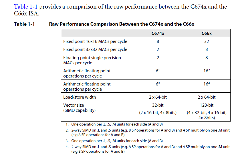
    The bit width is “Load/Store width 2 x 64 bit “ ( = 128 bit ) which is shown on table 1-1 in page 30 in sprugh7.pdf

    www.ti.com/lit/sprugh7

    The 32bit complex float number is 64 bit width.

    It would be 128 bit when two numbers which are multiplied.

    With this reason, it seems the data for only 1 multiple-accumulate can be loaded at one cycle.

    C66x has pipelines, however, it seems impossible to load the data at background


    Moreover, it is 256 bit width between internal memory, but it is between L1 and L2 transfer.

    The clock speed is slower than CPU clock.


    If it is assumed that coefficient of FIR is fit into the register which means small TAP numbers, it would be able to load 2 data for a multiple-accumulate at one cycle

    Is this a kind of figure?


    Of is DSPF_sp_fir_cplx “Fixed Point 16bit” ?


    When two complex float values which are multiple-accumulated are read from L1D every time, is it rate-limited?


    In addition, it outputs finally onto L1D with FIR calculation.

    If complex multiples are repeated again and again, it outputs onto L1D again and again.

    The load from L1D and the store to L1D are individually 2 x 64 bit width.

    If RD and WR to L1D occurs simultaneously, two accesses done by 1 clock if there is no bank conflict occurs.

    Are we correct?


    This is asked because we would like to make sure if the load is defined a rate-limited, the number of cycles must not be increased.

     
    Best regards,

    Hitoshi

  • Hitoshi-san,

    The C6000 architecture has 8 functional units that can execute an instruction each cycle.  There are two data units than are each capable of loading up to 64-bits of data from memory every cycle. These 64-bits can be 16-bit fixed point (so up to 4 16-bit values per side) or 32-bit fixed point (so up to 2 values per side) or 32-bit floating point (again up to two values per side).

    The C66x has 2 multiply units and each multiply unit is capable of 16 16-bit multiplies or 4 32-bit multiplies.

    Below is a table from the C66x instruction set guide SPRUGH7 that shows the load and multiply capability in terms of data size of the C66x.

    As you noted the load limitation is 64-bits per side. So for 16-bit fixed point math, I can only bring in 4 new pieces of data per clock cycle per side. And for 32-bit single precision floating point or 32-bit fixed point I can only bring in 2 32-bit values per side. So for real multiplies where I need new data every cycle, I am limited to 2 multiplies and adds but for complex multiplies where the data can be reused, we can increase the number of multiplies done.

    There also 4 other functional units that can be used for adds, logic expressions, compares or shifts. And these functional units can execute an instruction every cycle.

    So with these 8 functional units you can load data, multiply and add data every cycle. Where the pipeline comes in is you are not multiplying and adding the data that was loaded from memory this clock cycle. When loading from memory there is a four cycle latency before the data is ready in the register. So you are actually multiplying the data that was read four cycles ago. Similarly when you are doing an add, you are not adding the value to the multiply you did this clock cycle you are actually adding the data from the multiply of the a previous cycle (different data types have different latencies for the multiply to complete; table 5-2 in SPRUGH7 is a good place to start).

    Another question you had was on DSPF_sp_fir_cplx. That is a floating point function in DSPLIB. There are fixed point and floating point implementations of most common DSP functions (FIR, FFT, IIR, etc). When you see sp it means single precision floating point.

    I hope this answers your question on how it is possible to load data, do a multiply and add all in one cycle.

    If something is not clear, please let me know and I will try to clarify further.

    Jackie B.

  • Two more comments:
    1. Few years ago I made an example that shows how one can achieve 32G MAC on a single C66 core. Even though it is fixed point example (16-bit) floating point example will be similar (less performances of course). You can see it in e2e.ti.com/.../799811
    2. To demonstrate how to manipulate the cache for high performances I have an example of Cholsky decomposition. In this example I developed different code for very short (say 10x10) matrix as well as 128x128 matrix that will not fit inside L1D cache. So the example breaks the computations to minimize the cache misses. If you want I can send you the source code. It is a personal code and is not an official TI release, so it is only used as an example.

    Ran