This thread has been locked.

If you have a related question, please click the "Ask a related question" button in the top right corner. The newly created question will be automatically linked to this question.

problem of c6678 DSP MSI

hi TI professors, 

    I am using the altera fpga pcie communication with c6678 and the fpga work as EP and the dsp work as RC.I wanner realize the function is that the fpga control ad converter to acquisition data and save data to fifo. When fifo full will trigger the MSI which interrupt vector is 0, the dsp core0 receive the interrupt and remote configuration the fpga dma registers to transfer data from fpga fifo to dsp ddr3 sdram. When the dma trigger the dma transfer finished MSI which interrupt vector is 1, the dsp core0 receive the msi interrupt and notify core1 to process data.

    Now my problem is the fpga will trigger two msi interrupt which interrupt vector are 0 and 1, core0 receive two msi interrupt  but show common interrupt vector.I look the PCIE specification datasheet and I find  the MSI vector must continue and msi-x interrupt vector can discontinue.But the dsp core0 just receive msi vector is 0,8,16 and 24.It meaning is that fpga cannot send two msi interrupt to dsp.

    I am not sure if I am understanding this right. Can u give me some idea about dsp core0 receive two msi from fpga?

    think u!

  • Hello!
    IIRC, 32 MSI vectors supported and they spread evenly across all cores. So your Core0 receives vectors 0, 8, 16, 24, Core1 receives 1, 9, 17, 25, Core2 receives 2, 10, 18, 26 and so on. Thus, you have 4 MSI vector per core, which is more than enough to handle 'data ready' and 'transfer ready' events. Triggering multiple MSI is very simple: FPGA writes to 'msiIrq' required vector. So you can write 0 and 8 to trigger two events.
    I could not decipher the second para in you message, please elaborate.
    One thing to check is to see how many MSIs you've enabled during FPGA configuration. EP advertises number of MSIs it has and it's up to RC to enable them all, or restrict certain amount.
  • Hi again,

    One possible confusion might be that each core receives single event from PCIe subsystem like PCIe subsystem event #4 means there was MSI for the Core0, one of 0, 8, 16, 24, event #5 is MSI for Core1 with vector one of 1, 9, 17, 24 and so on. This event number could be a source for HWI triggering. However, in your ISR still you need to look at MSIn_IRQ_STATUS register to know which vector among 4 triggered this event.

    So again, Core0 can receive MSI vectors 0, 8, 16, 24. All four vectors trigger single event #4, and its up to user to read MSIn_IRQ_STATUS register and see which bit of four was set.

    Hope this helps, but please elaborate on your difficulty.

  • hi rrlagic,

        Thank u for your reply! I confiugrate the fifo full interrupt vector is 0 and the dma transfer finished interrupt vector is 8,but the MSI0_IRQ_STATUS register value is always 1 whatever the fpga send the interrupt vectors. The MULT_MSG_EN of MSI_CAP register value is 000 and the MULT_MSG_CAP value is 000. There is no way to change this value  in FPGA. I have tried to write 001 to MULT_MSG_EN but failed.I donn't know if this is the cause.

        In addition I wanner know if there is the example about the dsp core0 receive two msi interrupts.

  • Hello Sunny,

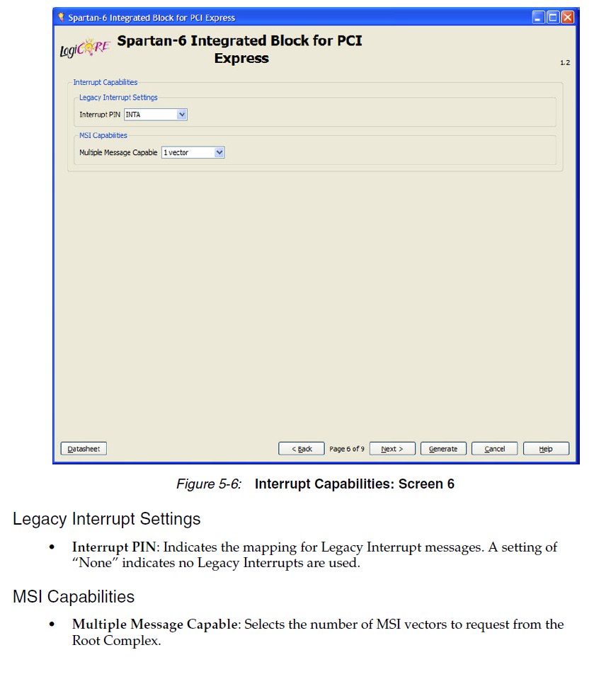
    As I understand the situation, EP advertises number of MSIs available through MSI multi message capability. Then its up to RC to read that value and request that amount or less. However, you say you see FPGA advertised zero as multimessage cap, meaning just one vector. I believe the key is on FPGA side. I am from Xilinx sandbox, so I could not guide you precisely. In my case when I was customizing PCIe IP Core, there was a page about number of MSI interrupts available, see the screenshot. You should be able to find similar parameter in your tools. After that you should be able to read greater value. Then enable multi message cap with something like

    {
            pcieMsiCapReg_t *reg = &MsiCap;
            uint32_t val = reg->raw = epCfg[(FPGA_CFG_MSI_CAP_OFFSET >> 2)];
    
            pcie_getbits(val, CSL_PCIE_CFG_SPACE_ENDPOINT_MSI_CAP_64BIT_EN,     reg->en64bit    );
            pcie_getbits(val, CSL_PCIE_CFG_SPACE_ENDPOINT_MSI_CAP_MULT_MSG_EN,  reg->multMsgEn  );
            pcie_getbits(val, CSL_PCIE_CFG_SPACE_ENDPOINT_MSI_CAP_MULT_MSG_CAP, reg->multMsgCap );
            pcie_getbits(val, CSL_PCIE_CFG_SPACE_ENDPOINT_MSI_CAP_MSI_EN,       reg->msiEn      );
            pcie_getbits(val, CSL_PCIE_CFG_SPACE_ENDPOINT_MSI_CAP_NEXT_CAP,     reg->nextCap    );
            pcie_getbits(val, CSL_PCIE_CFG_SPACE_ENDPOINT_MSI_CAP_CAP_ID,       reg->capId      );
        } /* pcie_read_msiCap_reg */
    
        /*
         * Endpoint advertize its MSI multi-vector capability in multMsgCap.
         * To enable some of those interrupts RC writes to multMsgEn.
         * Potentially we may restrict the number of allowed interrupts here.
         */
        MsiCap.multMsgEn = MsiCap.multMsgCap;   // Enable all available interrupts
        MsiCap.msiEn     = 1;                   // Enable MSI function
    
        {
            pcieMsiCapReg_t *reg = &MsiCap;
            uint32_t new_val = reg->raw;
            pcie_range_check_begin;
    
            pcie_setbits(new_val, CSL_PCIE_CFG_SPACE_ENDPOINT_MSI_CAP_64BIT_EN,    reg->en64bit     );
            pcie_setbits(new_val, CSL_PCIE_CFG_SPACE_ENDPOINT_MSI_CAP_MULT_MSG_EN, reg->multMsgEn   );
            pcie_setbits(new_val, CSL_PCIE_CFG_SPACE_ENDPOINT_MSI_CAP_MULT_MSG_CAP,reg->multMsgCap  );
            pcie_setbits(new_val, CSL_PCIE_CFG_SPACE_ENDPOINT_MSI_CAP_MSI_EN,      reg->msiEn       );
            pcie_setbits(new_val, CSL_PCIE_CFG_SPACE_ENDPOINT_MSI_CAP_NEXT_CAP,    reg->nextCap     );
            pcie_setbits(new_val, CSL_PCIE_CFG_SPACE_ENDPOINT_MSI_CAP_CAP_ID,      reg->capId       );
    
            epCfg[(FPGA_CFG_MSI_CAP_OFFSET >> 2)] = reg->raw = new_val;
        } /* pcie_write_msiCap_reg */

    At this point I should warn you again, that TI code provides some config space layout for remote EP. It is valid for TI devices, but let me assure you, it does not match at least Xilinx FPGAs. So in above code I had to use my own offsets like

    /*
     * Endpoint configuration space layout in FPGA is different from DSP's one,
     * so we have to define proper offsets and do not use LLD's values.
     * For clarity these offsets are byte addresses. Registers are accessed
     * as 32 bit values, so their dword offsets have to be adjusted as rsh(2).
     */
    #define FPGA_CFG_MSI_CAP_OFFSET             0x48
    #define FPGA_CFG_MSI_LOW32_ADDR_OFFSET      0x4C
    #define FPGA_CFG_MSI_UP32_ADDR_OFFSET       0x50
    #define FPGA_CFG_MSI_DATA_OFFSET            0x54
    #define FPGA_CFG_DEV_STAT_CTRL_OFFSET       0x60
    

    Be sure you are reading right registers and don't use TI's PCIe LLD for that purpose.