This thread has been locked.

If you have a related question, please click the "Ask a related question" button in the top right corner. The newly created question will be automatically linked to this question.

TMS320C6657: EMIF Address bit A23 Oscillating

Part Number: TMS320C6657

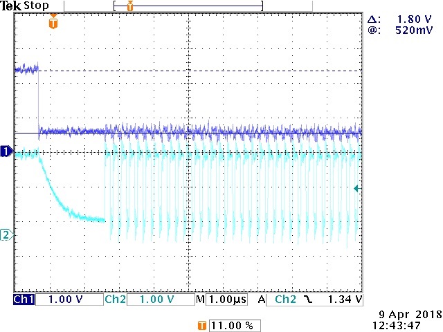
Hi, in our design, I am interfacing to a parallel NOR Flash (PC28F512P30EFA) via the EMIF16 bus. I can read the status register, however, when I go to do anything with the device ID or mfg ID, The Databus coming back from the part is oscillating with a pattern. The period is about 250ns. I've tracked it down to bit A23 oscillating at this rate during the read cycle. Only happens when I issue a 0x90 Read ID command prior to reading, Doesn't happen when I read flash or the status register. Program and Erase commands do not work.

The Board is routed incorrectly, with A23 going to Pin A25 on the Part, and not acting as bit 1. However, I wouldn't expect it to do this. Any Thoughts?

Brian Gonzales

  • Brian,

    I am wary of another board connection issue.  Are you looking at these signals with a scope or a logic analyzer?  Please post a scope (or LA) capture of both a good and a bad cycle.

    Tom

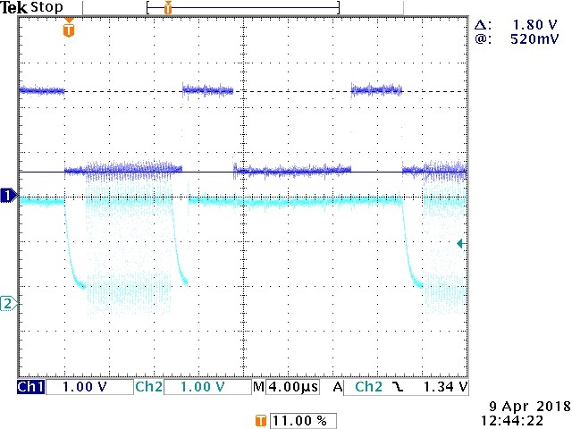
  • Here's A23 (A25 on the NOR Flash). Close up and further out. It's writing 0x90, then reading from address 0 (NOR flash base offset 0x78000000). If I put the NOR flash into array mode, this doesn't happen. 

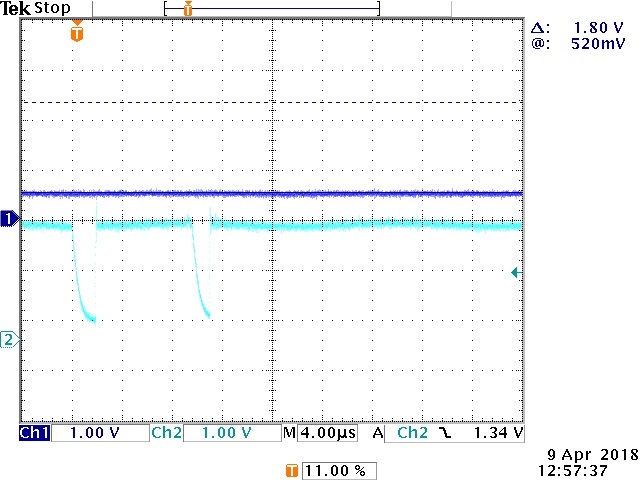
    WHen in Array Mode (write 0xFF), reading it looks like this: (address 23 should be 0).

  • Brian,

    I want to see what the other control signals are doing at the same time - also on a good versus bad cycle.  Please keep the cycle types identical.  Previously you said that reading a status register was successful but reading the device ID was not.  Please provide these comparative cycles but we need to see more control signals.  Also please be sure to provide a legend identifying the signals.

    Tom

  • I took some more screenshots. I do not have an external logic analyzer, so I cant show physical measurements of the rest of the bus. However, There is a FPGA attached that
    uses Address 0 to 21. It does not have access to 22 and 23.

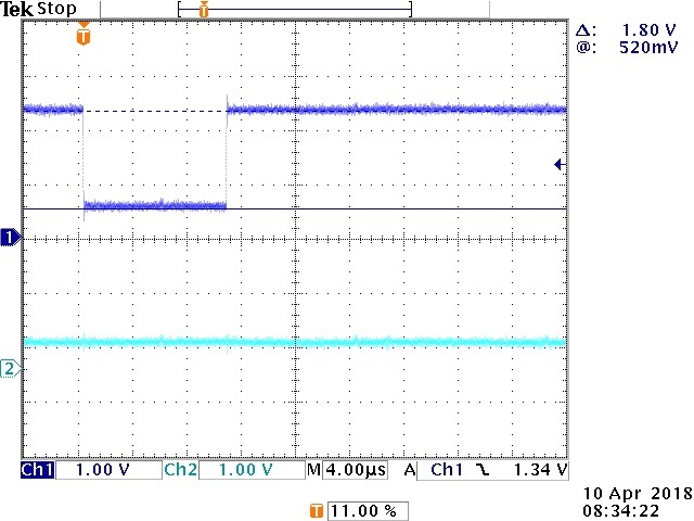
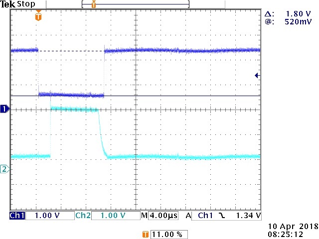
    For status read, I write a 0x70 to the NOR base address of 0x78000000. Then I read the base Address at 0x78000000. This results in these two waveforms (CE is Channel 1,
    A23 is Channel 2)

    Write:

    Read:

    Interesting thing is, A23 goes high for a read. Even though it is at the same base address as the write.

    Xilinx Chip Scope shows normal bus transaction (A23 not present on the plot). Here's a Status Write followed by a read on chipscope. TRIG0 is Address(21:0), TRIG1 is Data.

    Why is A23 going high during a Read at 0x78000000? Thats what is puzzling. 

  • Brian,

    The capture of A23 going high in the middle of the cycle does not have proper timing for an address bit.  I expect there is still an unexpected connection on the board to A23.  Can you probe around an find another signal that is changing simultaneous with A23?

    Tom

  • Good point.

    After some digging, and looking through a microscope, I realized I was probing DQ7, not A23 (They are neighbors on the BGA. My only access is using thin wire to edge BGA). The real A23 appears to be operating normally. DQ7 is high, since Status returns 0x80.

    So now, the issue is, why does our NOR flash return such garbled data. For the time being, this appears to be a flash issue.
  • Brian,
    Can I close this issue?
    Tom