This thread has been locked.

If you have a related question, please click the "Ask a related question" button in the top right corner. The newly created question will be automatically linked to this question.

Additional info for DM355 SPI Boot

I'm looking for a more detail explanation of SPI boot for DM355. Cypress offers SPI NOR flash but I am not sure if any of them will work with DM355 SPI boot.

Current description in "ARM subsystem ..." only mentions the layout of data in serial EEPROM/Flash. Is there any more info on what commands are sent to the memory chip and what is expected to come back so that I can verify compatibility.

Hope for a quick response.

  • Urgent help needed here!!!!

    I'm trying to figure out how SPI boot works. I've set the bootsel pins to 00 to boot from SPI. I do not see any activity on SPI0_CS, SPI0_CLK lines at reset. I was expecting to see the bootloader trying to read an external EEPROM.

    What is going on?

  • Hi,

    Our UBL only supports nand, nor, mmc/sd and uart boot modes.

    Can you pl. refer the below link for SPI boot support?

    regards,

    Anand

  • Really? Then what is section 11.2.1 is all about? It would not be there just for kicks and giggles, I assume.

    http://www.ti.com/lit/pdf/sprufb3

    When you say UBL, are you actually referring to RBL? Because I can write my own UBL and have it do what I want.

  • Hi Gennadiy,

    Below are few queries/reply -

    1) Please make sure that the probing is done on SPI0_CS and SPI0_CLK lines at the right time with proper triggers.

    2) Had you flashed any SPI UBL binary into the SPI device? please provide the SPI flash chip details.

    3) If you have JTAG access, diagnostic codes can be written to verify SPI read/write under IDE (Ex: Code Composer Studio). By this, hardware and communication can be verified.

    Regards

    Gajanan

     www.pathpartnertech.com

  • I'm probing on SPI0 pins. There is no activity on those pins at the time of reset. If I've add SPI0 communication to my SD-card boot code, my scope triggers and I see the lines toggle. But when I switch to SPI boot, nothing happens.
    Only after checking errata I found out that SPI boot is only available on 1.4 chip revision. That was a bummer. If only they had that in the datasheet, it would've saved me a whole lot of time. My EVM has old revision in it. I cannot figure out how the SPI boot works.
    Can anybody answer my first question? I need to know what commands are sent during SPI boot and what is expected back. Also, what commands does DM355 send to set external chip to 24/16 bit mode.

  • Hi Gennadiy,

              I am not sure about the exact commands used to set the external chip to 24/16 bit mode. But more details can be grabbed from SPI Controller driver in kernel or from chip-set datasheet. All the chip-set datasheets will have specific commands (maybe same across supporting chip-sets) for specific operations (Ex: read/write). So you should understand the operations from SPI Boot -Detailed Flow and expect those numbers while probing.


    Regards

    Gajanan

     www.pathpartnertech.com

  • The SPI Boot you refer to, says that it first tries 24 bit address and reads the first byte. If I had to, I would assume that the address is sent MSB first. Address for the first byte would be 000008h. If we happened to have a 16-bit addressable device connected, it would recognize only the first 2 bytes of the address which would be 0000 instead of 0008. As the result, the chip would return data from a different address. Typically, first 8 bytes are used for MAC address and thus could be anything. Because of that I am not sure how the chip can read the first byte and determine if it has to switch to 16-bit addressing mode. Am I missing something? Does it do some other trick to determine the addressing mode? Does it send the address LSB first?
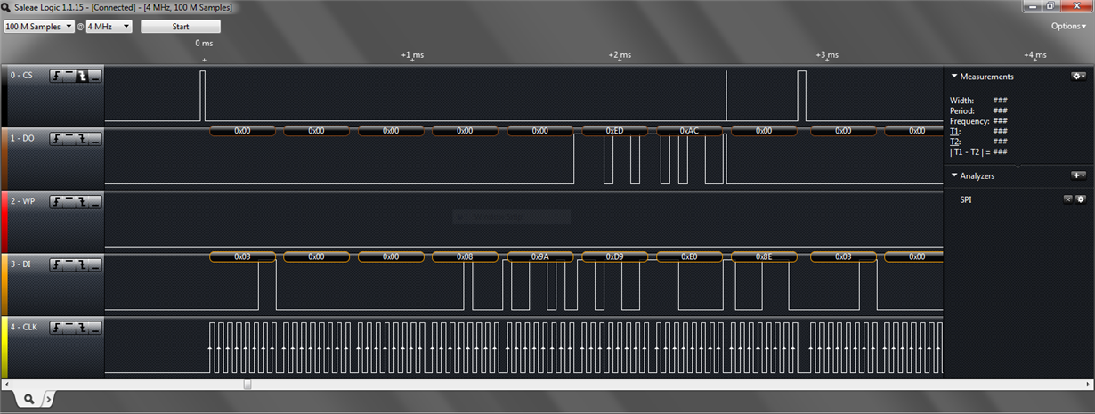
  • Well... that did not go so well. It looks like SPI boot does not work or appears to be broken. I had to find it out the hard way after making a prototype circuit board relying on SPI boot. Here is how DM355 attempts to read the SPI flash.

    1. It attempts to read the flash in 24 bit mode. But the darn thing appears to have a bug in the code as described in the errata on page 21 (SPI Master Mode: Extra Step Required to Use CSHOLD). That glitch (that thing stick on CS line around 2.5ms marker) causes the SPI memory to start another command.

    2. Among many things what is not clear is why it is reading only the first 4 bytes. The glitch appears because the code attempts to read the last byte despite the fact that the previous bytes were all correct. It is outside of the screen in the picture above but the processor later tries to read the SPI memory in 16 bit mode. It reads the whole 24 bytes even though the first bytes are not even close to contain the magic number. Why is reading in 24-bit mode different? Why reading only 4 bytes? What does it do next? Do I need to use a different magic number?

    We use a 24-bit addressable SPI flash. I need to make it work. Tell me how. I also need clarification on items 1 and 2.