This thread has been locked.

If you have a related question, please click the "Ask a related question" button in the top right corner. The newly created question will be automatically linked to this question.

DM8148 Debug

Other Parts Discussed in Thread: CCSTUDIO

Hello,

              Making DM8148 PCB, there has been a few bad pcb, when the boot mode using Nand flash output without any message, when uart mode can output ccccc ...., but all of the output voltage, reset signal, the oscillator output frequency outputs normal, so can connect using Jtag and ccs to debug it?

  • aska huang said:
    so can connect using Jtag and ccs to debug it?

    Yes, I think you can use the JTAG, see the below e2e thread for more info:

    http://e2e.ti.com/support/dsp/davinci_digital_media_processors/f/716/t/331762.aspx

    See also the below wiki pages:

    http://processors.wiki.ti.com/index.php/DM814x_Overview#Schematics_.26_PCB_support.3B_Symbols.2C_Footprints.2C_and_Simulation_Models

    http://processors.wiki.ti.com/index.php/Debug_Tips_for_DM81xx_Boot_Fail

    http://processors.wiki.ti.com/index.php/DM814x_Hardware_Design_Guide

    http://processors.wiki.ti.com/index.php/DM814x_Software_Design_Guide#Debugging

    BR
    Pavel

  • Hi Pavel,

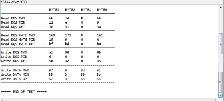
                       Thanks for you reply,I have followed the "http://processors.wiki.ti.com/index.php?title=TI814x-DDR3-Init-U-Boot" get under result, so DDR problems? Byte1 DQS which are 0, which as determine which one DDR memory problems? Then how should I do? Thanks

  • Aska,

    SW leveling process is not intended to diagnose a non-working DDR interface. It is only intended for fine tuning the DDR PHY when the DDR interface is functionally working.  It is meaningless to proceed further with SW leveling if the memory access is not working.

    Can you first check and verify that your DDR3 memory access is working. Try with lower DDR3 frequency and refer to the below HW diagnostic test:

    CCS_Code_BB/src/CCS_Test_code/Base_Board/DDR3

    This CCS test application validates the DDR memory for its ability to perform write access; read access and data storing ability. The test application writes a known pattern into the entire memory and then reads back the same. The known pattern written into the memory is the incremental hexadecimal numbers. After   writing to the entire memory area, this application reads them back and validates the data read. If the data read does not match the expected pattern, this test is declared failed. It is declared pass otherwise.

    This HW diagnostic test is for the DM814x/AM387x TI EVM (see link below) so you might need to adjust it for your specific board.

    Can you also check if your u-boot hang/stuck at the config_ti814x_ddr() function in file u-boot/board/ti/ti8148/evm.c?

    http://processors.wiki.ti.com/index.php/Understanding_u-boot-min_startup_for_DM814x

    board/ti/ti8148/evm.c

    Contains s_init() function which sets up PLLs, DDR (only when running from SRAM), and pin muxing


    /*
    * early system init of muxing and clocks.
    */
    void s_init(u32 in_ddr)
    {
    .................
    #if defined(CONFIG_TI814X_CONFIG_DDR)
    if (!in_ddr)
    config_ti814x_ddr(); /* Do DDR settings */
    #endif
    }

    BR
    Pavel

  • Dear Pavel,

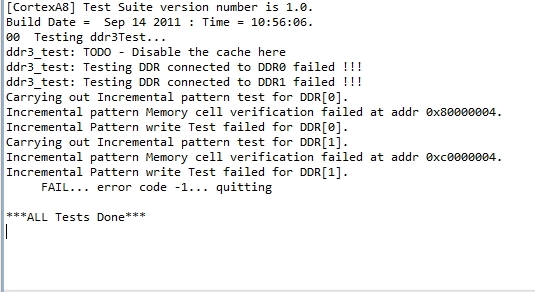
                            Thank you for your detailed reply, I have run ddr3 test, get under a result, will be able to know ddr0 & ddr1 failed, it was side of the DM8148 emif a problem, or DDR3 Memory problems? Which one ddr3 memory problems? Thanks.

  • Aska,

    aska huang said:
    will be able to know ddr0 & ddr1 failed

    Both DDR0 and DDR1 failed.

    Did you run the GEL scripts before running the DDR3 test?

    Procudure
    ----------
    This test application assumes the DDR controller initialization as well as all the PLL initialization is already carried out by the GEL scripts.  
                      1. PG 2.x DM814X --> ALL_ADPLL_CLOCKS_ENABLE_API  
                      2. PG 2.x DM814X --> DDR3_EMIF0_EMIF1_Config_Full_leveling
     
    load "BB_021_DDR3_TEST.out" file and run.

    Can you also check if your u-boot hang/stuck at the config_ti814x_ddr() function in file u-boot/board/ti/ti8148/evm.c?

    BR
    Pavel

  • Aska,

    Below is what I have when I run the GEL scripts and DDR3 test on the DM814x TI EVM:

    CortexA8: Output:      ****  CENTAURUS2 ALL ADPLL INIT IS In Progress .........
    CortexA8: GEL Output:      MODENA ADPLLJ CLKOUT  value is  = 600
    CortexA8: GEL Output:      L3  ADPLLJ CLKOUT  value is  = 200
    CortexA8: GEL Output:      DSP ADPLLJ CLKOUT  value is  = 500
    CortexA8: GEL Output:      DSS ADPLLJ CLKOUT  value is  = 200
    CortexA8: GEL Output:      ISS ADPLLJ CLKOUT  value is  = 200
    CortexA8: GEL Output:      IVA ADPLLJ CLKOUT  value is  = 266
    CortexA8: GEL Output:      SGX ADPLLJ CLKOUT  value is  = 200
    CortexA8: GEL Output:      USB ADPLLJ CLKOUT  value is  = 192
    CortexA8: GEL Output:      VIDEO-0 ADPLLJ CLKOUT  value is  = 54
    CortexA8: GEL Output:      VIDEO-1 ADPLLJ CLKOUT  value is  = 148
    CortexA8: GEL Output:      VIDEO-2/HDMI ADPLLJ CLKOUT  value is  = 148
    CortexA8: GEL Output:      DDR ADPLLJ CLKOUT  value is  = 333
    CortexA8: GEL Output:      AUDIO ADPLLJ CLKOUT  value is  = 200
    CortexA8: Output:      **** SATA PLL INIT IS In Progress Please wait .....
    CortexA8: Output:      **** SATA PLL INIT IS In DONE *****************
    CortexA8: Output:      **** PCIE PLL INIT IS In Progress Please wait .....
    CortexA8: Output:      **** PCIE PLL INIT IS In DONE *****************
    CortexA8: Output:      ****  CENTAURUS2 ALL ADPLL INIT IS  Done **************
    CortexA8: Output:      ****  CENTAURUS2 DDR3 Full_leveling EMIF0 and EMIF1 configuration in progress.........
    CortexA8: Output:     Busy reading back DMM registers Please wait ...
    CortexA8: Output:     DMM register read successfully  
    CortexA8: Output:      ****  CENTAURUS2 DDR3 Full_leveling EMIF0 and EMIF1 configuration is DONE ****

    [CortexA8] Test Suite version number is 1.0.
    Build Date =  Sep 14 2011 : Time = 10:56:06.
    00  Testing ddr3Test...
    ddr3_test: TODO - Disable the cache here
    Carrying out Incremental pattern test for DDR[0].
    Carrying out Incremental pattern test for DDR[1].
        PASS

    ***ALL Tests Done***

    Please compare your DDR3 design with the DM814x TI EVM DDR3 design.

    BR
    Pavel

  • Hi Pavel,

                         I missed loaded GEL, please help confirmation step.

                         The result is Pass, but testing DDR connected to DDR0 failed,

                          so could you suggestion action of next step? thanks!

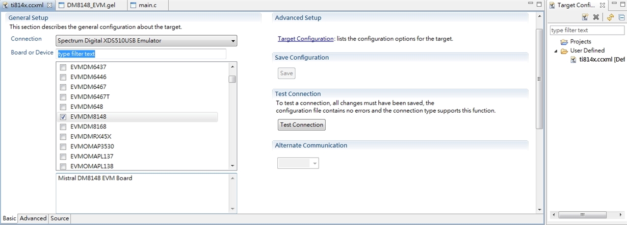
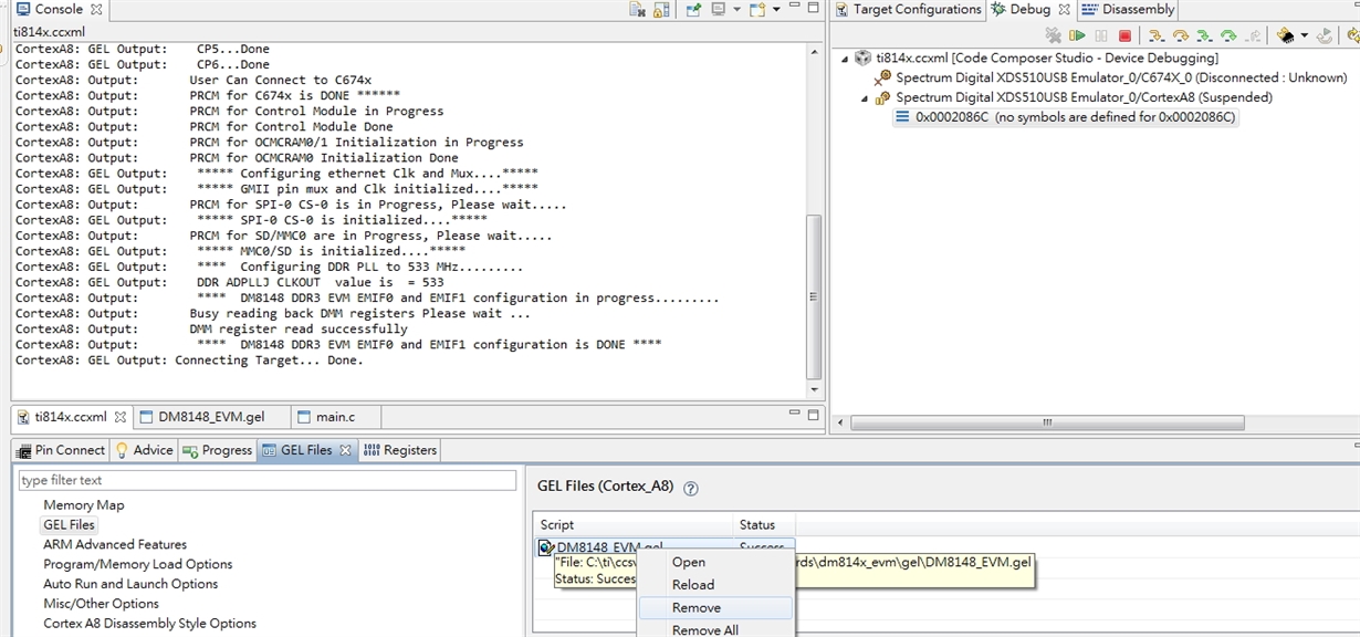
    Step1:Select device: EVMDM8148

    Step2:Connect Target CortexA8

    Step3:Remove DM8148_evm.GEL

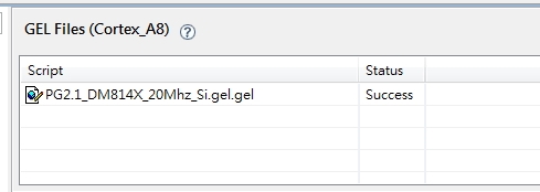
    Step4:Load CCS_Code_BB>src>CCS_Test_code>GEL>PG2.1_DM814X_20MHz_Si.gel.gel

    Step5:run scripts

                1.ALL_ADPLL_CLOCKS_ENABLE_API

                2.DDR3_EMIF0_EMIF1_Config_Full_leveling

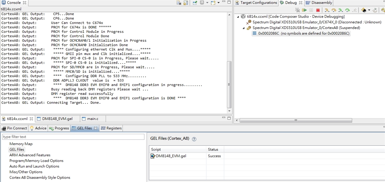
    CortexA8: GEL Output:
    Connecting Target...
    CortexA8: Output:      ****  DM8148 ALL ADPLL INIT IS In Progress .........
    CortexA8: GEL Output:      A8 ADPLLJ CLKOUT  value is  = 600
    CortexA8: GEL Output:      L3  ADPLLJ CLKOUT  value is  = 200
    CortexA8: GEL Output:      DSP ADPLLJ CLKOUT  value is  = 500
    CortexA8: GEL Output:      DSS ADPLLJ CLKOUT  value is  = 200
    CortexA8: GEL Output:      HDVICP ADPLLJ CLKOUT  value is  = 266
    CortexA8: GEL Output:      SGX ADPLLJ CLKOUT  value is  = 200
    CortexA8: GEL Output:      USB ADPLLJ CLKOUT  value is  = 192
    CortexA8: GEL Output:      VIDEO-0 ADPLLJ CLKOUT  value is  = 54
    CortexA8: GEL Output:      VIDEO-1 ADPLLJ CLKOUT  value is  = 148
    CortexA8: GEL Output:      VIDEO-2/HDMI ADPLLJ CLKOUT  value is  = 148
    CortexA8: GEL Output:      AUDIO ADPLLJ CLKOUT  value is  = 200
    CortexA8: Output:      ****  DM8148 ALL ADPLL INIT IS  Done **************
    CortexA8: Output:     PRCM for C674x is in Progress, Please wait.....  
    CortexA8: GEL Output:      CP0...Done
    CortexA8: GEL Output:      CP1...Done
    CortexA8: GEL Output:      CP2...Done
    CortexA8: GEL Output:      CP3...Done
    CortexA8: GEL Output:      CP4...Done
    CortexA8: GEL Output:      CP5...Done
    CortexA8: GEL Output:      CP6...Done
    CortexA8: Output:     User Can Connect to C674x   
    CortexA8: Output:     PRCM for C674x is DONE ******  
    CortexA8: Output:     PRCM for Control Module in Progress
    CortexA8: Output:     PRCM for Control Module Done
    CortexA8: Output:     PRCM for OCMCRAM0/1 Initialization in Progress
    CortexA8: Output:     PRCM for OCMCRAM0 Initialization Done
    CortexA8: GEL Output:      ***** Configuring ethernet Clk and Mux....*****
    CortexA8: GEL Output:      ***** GMII pin mux and Clk initialized....*****
    CortexA8: Output:     PRCM for SPI-0 CS-0 is in Progress, Please wait.....  
    CortexA8: GEL Output:      ***** SPI-0 CS-0 is initialized....*****
    CortexA8: Output:     PRCM for SD/MMC0 are in Progress, Please wait.....  
    CortexA8: GEL Output:      ***** MMC0/SD is initialized....*****
    CortexA8: GEL Output:      ****  Configuring DDR PLL to 533 MHz.........
    CortexA8: GEL Output:      DDR ADPLLJ CLKOUT  value is  = 533
    CortexA8: Output:      ****  DM8148 DDR3 EVM EMIF0 and EMIF1 configuration in progress.........
    CortexA8: Output:     Busy reading back DMM registers Please wait ...
    CortexA8: Output:     DMM register read successfully  
    CortexA8: Output:      ****  DM8148 DDR3 EVM EMIF0 and EMIF1 configuration is DONE ****
    CortexA8: GEL Output: Connecting Target... Done.

    CortexA8: Output:      ****  DM814X2 ALL ADPLL INIT IS In Progress .........
    CortexA8: GEL Output:      MODENA ADPLLJ CLKOUT  value is  = 600
    CortexA8: GEL Output:      L3  ADPLLJ CLKOUT  value is  = 200
    CortexA8: GEL Output:      DSP ADPLLJ CLKOUT  value is  = 500
    CortexA8: GEL Output:      DSS ADPLLJ CLKOUT  value is  = 200
    CortexA8: GEL Output:      ISS ADPLLJ CLKOUT  value is  = 400
    CortexA8: GEL Output:      IVA ADPLLJ CLKOUT  value is  = 266
    CortexA8: GEL Output:      SGX ADPLLJ CLKOUT  value is  = 200
    CortexA8: GEL Output:      USB ADPLLJ CLKOUT  value is  = 192
    CortexA8: GEL Output:      VIDEO-0 ADPLLJ CLKOUT  value is  = 54
    CortexA8: GEL Output:      VIDEO-1 ADPLLJ CLKOUT  value is  = 148
    CortexA8: GEL Output:      VIDEO-2/HDMI ADPLLJ CLKOUT  value is  = 148
    CortexA8: GEL Output:      DDR ADPLLJ CLKOUT  value is  = 333
    CortexA8: GEL Output:      AUDIO ADPLLJ CLKOUT  value is  = 200
    CortexA8: Output:      **** SATA PLL INIT IS In Progress Please wait .....
    CortexA8: Output:      **** SATA PLL INIT IS In DONE *****************
    CortexA8: GEL Output: exiting pll setup

    CortexA8: GEL Output: CONFIGURE PRCM CLOCKS of EMAC in progress

    CortexA8: GEL Output: PRCM CLOCKS of EMAC  is complete

    CortexA8: Output:      ****  DM814X2 ALL ADPLL INIT IS  Done **************
    CortexA8: Output:      ****  DM814X2 DDR3 Full_leveling EMIF0 and EMIF1 configuration in progress.........
    CortexA8: Output:     Busy reading back DMM registers Please wait ...
    CortexA8: Output:     DMM register read successfully  
    CortexA8: Output:      ****  DM814X2 DDR3 Full_leveling EMIF0 and EMIF1 configuration is DONE ****

    Step6:Load CCS_Code_BB>src>CCS_Test_code>Base_Board>DDR3>Debug>BB_021_DDR3_TEST.out

    [CortexA8] Test Suite version number is 1.0.
    Build Date =  Sep 14 2011 : Time = 10:56:06.
    00  Testing ddr3Test...
    ddr3_test: TODO - Disable the cache here
    ddr3_test: Testing DDR connected to DDR0 failed !!!
    Carrying out Incremental pattern test for DDR[0].
    Incremental pattern Memory cell verification failed at addr 0x80000004.
    Incremental Pattern write Test failed for DDR[0].
    Carrying out Incremental pattern test for DDR[1].
        PASS

    ***ALL Tests Done***


  • Aska,

    aska huang said:
    Step1:Select device: EVMDM8148

    From what I understand, you are using DM814x custom board, not DM8148 TI EVM. Can you try with DM814x (instead of EVMDM8148)?

    aska huang said:
    Step4:Load CCS_Code_BB>src>CCS_Test_code>GEL>PG2.1_DM814X_20MHz_Si.gel.gel

    Can you try with DM814x_PG2.x.gel (located at DM814x_gel/) instead of the PG2.1_DM814X_20MHz_Si.gel.gel

    BR
    Pavel

  • Pavel,

               
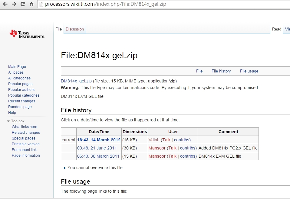
    I use DM814x replace EVMDM8148, then use this link "http://processors.wiki.ti.com/index.php/File:DM814x_gel.zip, download the second file (09:48, 21 June 2011), because only this one have DM814x PG2.x GEL file, but the run "ALL_ADPLL_CLOCKS_ENABLE_API" scripts will have been in this step, could you help to confirm, thank you.

  • Aska,

    aska huang said:
    but the run "ALL_ADPLL_CLOCKS_ENABLE_API" scripts will have been in this step, could you help to confirm, thank you.

    I am not sure what exactly should I confirm, thanks you.

    BR
    Pavel

  • I am attaching the GEL file I use

    DM814x_PG2.x.gel

  • Pavel,

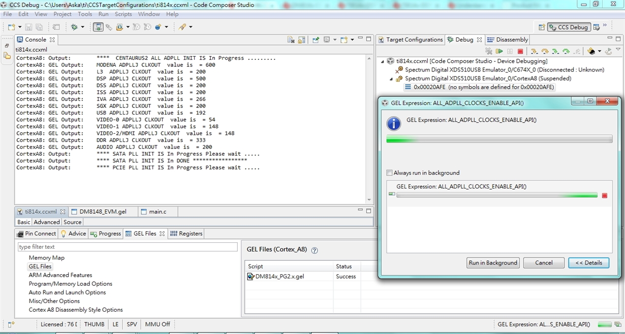
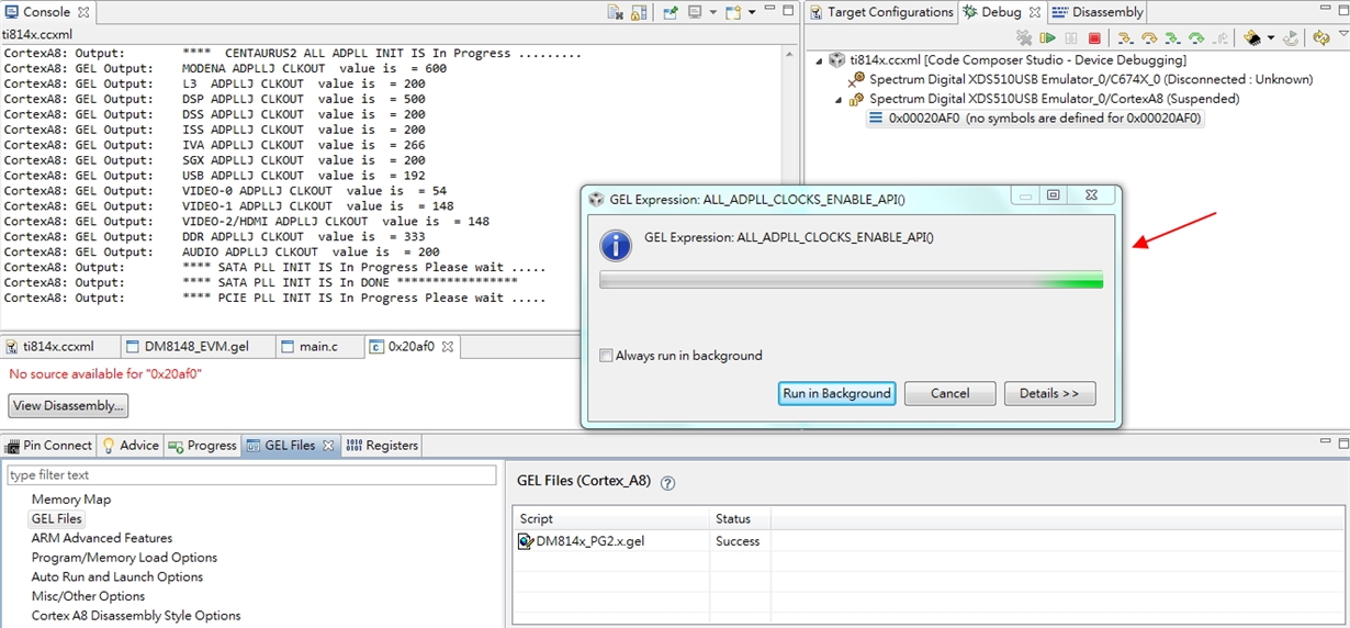
               I used attaching the GEL file, but after 10 minutes still not done,

                you know what the happen problem? Thanks!

  • Aska,

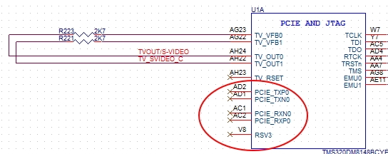
    It seems to me that the flow hang at the PCIe PLL init function cmdPCIEPLL(). Do you have PCIe in your custom board?

    BR
    Pavel
  • Pavel,

                   I have not use the interface of pcie, this interface is now left unconnected.thanks.

  • Aska,

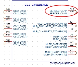
    What about the SERDES_CLKP and SERDES_CLKN pins?

    Can you comment the PCIe init function in GEL file, like below and try.

    PLL_SETUP(){
    ...
    //cmdPCIEPLL();
    }

    Regards,
    Pavel
  • Pavel,

                 The SERDES_CLKP and SERDES_CLKN pins is left unconnected.
    I have a comment the PCIe init function in GEL file, "ALL_ADPLL_CLOCKS_ENABLE_API" scripts can be done,

    Run the "BB_021_DDR3_TEST.out" result is pass, but the DDR [0] is show failed,
    so, how do you think? Thanks.

    Scripts:

    CortexA8: Output:      ****  CENTAURUS2 ALL ADPLL INIT IS In Progress .........
    CortexA8: GEL Output:      MODENA ADPLLJ CLKOUT  value is  = 600
    CortexA8: GEL Output:      L3  ADPLLJ CLKOUT  value is  = 200
    CortexA8: GEL Output:      DSP ADPLLJ CLKOUT  value is  = 500
    CortexA8: GEL Output:      DSS ADPLLJ CLKOUT  value is  = 200
    CortexA8: GEL Output:      ISS ADPLLJ CLKOUT  value is  = 200
    CortexA8: GEL Output:      IVA ADPLLJ CLKOUT  value is  = 266
    CortexA8: GEL Output:      SGX ADPLLJ CLKOUT  value is  = 200
    CortexA8: GEL Output:      USB ADPLLJ CLKOUT  value is  = 192
    CortexA8: GEL Output:      VIDEO-0 ADPLLJ CLKOUT  value is  = 54
    CortexA8: GEL Output:      VIDEO-1 ADPLLJ CLKOUT  value is  = 148
    CortexA8: GEL Output:      VIDEO-2/HDMI ADPLLJ CLKOUT  value is  = 148
    CortexA8: GEL Output:      DDR ADPLLJ CLKOUT  value is  = 333
    CortexA8: GEL Output:      AUDIO ADPLLJ CLKOUT  value is  = 200
    CortexA8: Output:      **** SATA PLL INIT IS In Progress Please wait .....
    CortexA8: Output:      **** SATA PLL INIT IS In DONE *****************
    CortexA8: Output:      ****  CENTAURUS2 ALL ADPLL INIT IS  Done **************
    CortexA8: Output:      ****  CENTAURUS2 DDR3 Full_leveling EMIF0 and EMIF1 configuration in progress.........
    CortexA8: Output:     Busy reading back DMM registers Please wait ...
    CortexA8: Output:     DMM register read successfully  
    CortexA8: Output:      ****  CENTAURUS2 DDR3 Full_leveling EMIF0 and EMIF1 configuration is DONE ****

    Load "BB_021_DDR3_TEST.out":

    [CortexA8] Test Suite version number is 1.0.
    Build Date =  Sep 14 2011 : Time = 10:56:06.
    00  Testing ddr3Test...
    ddr3_test: TODO - Disable the cache here
    ddr3_test: Testing DDR connected to DDR0 failed !!!
    Carrying out Incremental pattern test for DDR[0].
    Incremental pattern Memory cell verification failed at addr 0x80080004.
    Incremental Pattern write Test failed for DDR[0].
    Carrying out Incremental pattern test for DDR[1].
        PASS

    ***ALL Tests Done***

  • Aska,

    aska huang said:
    but the DDR [0] is show failed

    aska huang said:
    ddr3_test: Testing DDR connected to DDR0 failed !!!
    Carrying out Incremental pattern test for DDR[0].
    Incremental pattern Memory cell verification failed at addr 0x80080004.
    Incremental Pattern write Test failed for DDR[0].

    I think there is something wrong in your DDR3 HW design. In DM814x TI EVM we have 512MB on DDR3_0 and 512MB on DDR3_1. 32-bit DDR3 interface is used for both DDR3_0 and DDR3_1. Four 8-bit DDR3 chips (MT41J128M8JP-125) are connected to DDR3_0. See DM814x TI EVM schematics and DM814x datasheet, Figure 8-55. 32-Bit, One-Bank DDR3 Interface Schematic Using Four 8-Bit DDR3 Devices

    How about your DM814x custom board DDR3 HW design?

    BR
    Pavel

  • Pavel,

                    There are two boards had a similar problem (DDR problem), but the other board is good.
    My custom board DDR3 HW design using two 16bit DDR3 (H5TQ2G63DFR) chips  connected DDR3 [0] and use two 16bit DDR3 (H5TQ2G63DFR) chips connected DDR3 [1], so there will be a problem? Thank you!

  • Aska,

    aska huang said:
    My custom board DDR3 HW design using two 16bit DDR3 (H5TQ2G63DFR) chips  connected DDR3 [0] and use two 16bit DDR3 (H5TQ2G63DFR) chips connected DDR3 [1], so there will be a problem?

    This is valid configuration, if handled properly of course. See DM814x datasheet, Figure 8-54. 32-Bit, One-Bank DDR3 Interface Schematic Using Two 16-Bit DDR3 Devices

    aska huang said:
    There are two boards had a similar problem (DDR problem), but the other board is good.

    Are these boards (working and failing) have the same DDR3 HW design (two 16-bit chips on DDR3_0 and two 16-bit chips on DDR3_1)?

    Best regards,
    Pavel

  • Pavel,
    Yes,these boards (working and failing) have the same DDR3 HW design (two 16-bit chips on DDR3_0 and two 16-bit chips on DDR3_1),So, do not know what causes failed.thanks!
  • Aska,

    aska huang said:
    Yes,these boards (working and failing) have the same DDR3 HW design (two 16-bit chips on DDR3_0 and two 16-bit chips on DDR3_1),So, do not know what causes failed.thanks!

    Can you run successfully the DDR3 CCStudio test code on the working board? Is it successful there? Can you boot the working board with the default u-boot from DM814x EZSDK?

    When one SW runs fine on one HW, and the same SW fails on other HW, this is most often indication of a HW malfunction and revision of the failing HW is required, use the below pointers as reference:

    - the working board schematics

    - the DM814x TI EVM schematics

    - DM814x datasheet

    -

    -

    -

    -

    BR
    Pavel

  • Pavel,

                 Yes, the run DDR3 CCStudio test code on the working board, result is pass.
    so, I think the failure of two boards are Incremental pattern Memory cell verification failed at addr 0x80000004, said the DDR memory problems? So, should replace DM8148 ic or DDR[0] memory (connect two chips , which one should be replaced?) If replacement parts will then fix? how do you think? Thanks.