This thread has been locked.

If you have a related question, please click the "Ask a related question" button in the top right corner. The newly created question will be automatically linked to this question.

Issue with AM1808 DDR2

Other Parts Discussed in Thread: AM1808

Hi,

Our customer is using DDR2 with AM1808,
and few of the custom boards has issue(system crash) related to DDR2.

They see the data on the DDR changing constantly even when
the CPU and clocks are OFF. But restores with a reset on DDR PHY.
The DDR is configured in point-to-point, without any external termination.

The system crashes if they use weak drive strength,
but if they use the normal drive strength, the system works normally
with significant overshoot/undershoot.

We are trying to get the customer's schematics to check if it as per the
datasheet guidelines.

Meanwhile if possible could you please comment on the below behaviour.

1.As mentioned above the DDR contents are restored to normal with a
reset on DDR PHY, what could be the reason for DDR contents restored to normal
with a reset on DDR PHY.

2.When they change the Read latency(RL) value on the DDR PHY Control Register 1 (DRPYC1R),
few working boards also started showing this crash behaviour, does it mean the
timings of the DDR memory and the board is not tuned correctly?

3.It was written on the E2E that VTP calibration is done in the ROM Bootloader
hence they don't execute the VTP calibration in their program(bootloader).
Is it necessary to do the VTP calibration in user program(like u-boot) and what could
be the effect of disabling VTP?
note: they tried to add VTP calibration code but still the issue exists.

4.They have found that touching a Probe(1pF) on DQS1 pin causes a system crash.
Does it indicates a wrong soldering or wrong via?

Regards
Prad

  • Hello Prad,

    I want you to first ensure that the customer has followed all the schematics and layout guidelines for DDR interface given in the device datasheet.

    If the system crash with weak drive strength without any terminations, there might be an issue with PCB routing. However normal drive strength may be used given that the JEDEC overshoot requirements are still met.

    http://processors.wiki.ti.com/index.php/DDR_Routing_Checklist#DDR2.2FmDDR.2FDDR3_Routing_Checklist

    http://processors.wiki.ti.com/index.php/DDR_Interface_Drive_Strength


    Answering to your questions,

    1. I hope you are referring this behavior as system crash. How did you verify this behavior ? 

    2. The issue is likely due to timing problem. Please check the routing and also verify the control register settings with the spreadsheet available in below link.

    http://processors.wiki.ti.com/index.php/Programming_mDDR/DDR2_EMIF_on_OMAP-L1x/C674x 

    3. The VTP calibration is performed whenever the DDR initialization sequence is executed. It is not required to do the calibration again in the user program and you cannot skip the VTP calibration since it controls the output impedance of DDR IO. Please refer section 14.2.12 in AM1808 TRM.

    http://www.ti.com/lit/ug/spruh82a/spruh82a.pdf

    4. Check the PCB board file and assembly. Are you seeing this issue only on DQS1 or other pins also ?

    Regards,

    Senthil

  • Hi Senthil,

    Thank you so much for the quick reply.
    Your information is very helpful.

    Regarding the questions,

    1.This issue is confirmed with a Test program and a Trace debugger.

    2.We shall check as per your suggestion.

    3.We need one clarification regarding the VTP Calibration, .
    Is the VTP calibration done by the ROM-Bootloader automatically or it should be done
    through the user program(like U-boot) when initializing the DDR memory.

    4.We shall check if this occurs in other pins also.


    Regards
    Prad

  • Hi Prad,

    3.We need one clarification regarding the VTP Calibration, .
    Is the VTP calibration done by the ROM-Bootloader automatically or it should be done
    through the user program(like U-boot) when initializing the DDR memory.

    u-boot/arch/arm/cpu/arm926ejs/davinci/da850_lowlevel.c

    u-boot/include/configs/da850evm.h

    It depends whether you have declared "CONFIG_SYS_DA850_DDR_INIT" in u-boot config file.

    If you are not declared then VTP calibration will not be done.

    Ex:

    #define CONFIG_SYS_DA850_DDR_INIT

  • Thank you for the information,

    I shall Verify(Close) this post once we solve the issue.

    Regards
    Prad

  • Hi Senthil, Titus

    Could you please clarify one more question on DDR2 Drive settings.

    The below E2E mentions that 
    "When no termination is used, the DDR2/mDDR devices must be programmed to operate in 60% strength mode"
    http://e2e.ti.com/support/dsp/omap_applications_processors/f/42/t/261650.aspx

    As mentioned above in our case the DDR (MT47H64M16HR-3IT-H) is configured in point-to-point, without any external termination,so we are setting the drive strength through DDRDRIVE[1:0] bits of SDCR register(as per the TRM)

    But in the above E2E it is also mentoined that "the programming is done on the DDR memory
    device, not on AM1808".
    We don't understand how do we program the drive strenght of the DDR memory,
    is it done through the AM1808 command?

    Meanwhile, we have some details about the overshoot/undershoot voltage on DQS1 line.
    As mentioned above the the system crashes if they use weak drive strength,
    and if they use the normal drive strength, the system works normally with significant overshoot/undershoot.
    We have found the overshoot/undershoot voltage is about 0.5V (i.e 1.8V+0.5)
    which is out of spec with regards to the AM1808 datasheet but within spec with regards to JESD79-2A standard.

    Regards
    Prad

  • Hello Prad,

    But in the above E2E it is also mentoined that "the programming is done on the DDR memory 
    device, not on AM1808". 
    We don't understand how do we program the drive strenght of the DDR memory,
    is it done through the AM1808 command?

    Yes, the drive strength can be programmed in DDR memory using EMRS command. Please refer section14.2.13 in AM1808 TRM.

    http://www.ti.com/lit/ug/spruh82a/spruh82a.pdf

    We have found the overshoot/undershoot voltage is about 0.5V (i.e 1.8V+0.5) 
    which is out of spec with regards to the AM1808 datasheet but within spec with regards to JESD79-2A standard.

    Could you please point out where you are referring overshoot specifications in device datasheet. However, if the overshoot is within JESD79-2A standard spec, the normal drive strength may be used.


    Regards,
    Senthil


  • Hi Senthil,

    Thank you so much for the information.

    Regarding the overshoot specification I was referring to a wrong data
    page 64 "Input voltage (VI) ranges". I am sorry for the confusion.

    But I found below statement in the Datasheet and understood the DDR I/O's
    overshoot/undershoot spec is as per JESD79-2A standard.
    "DDR2/mDDR IOs are 1.8V IOs and adhere to the JESD79-2A standard."

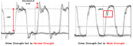
    Meanwhile we have received below waveform measured on the DQS1 line,
    with Drive strength set to Normal and Weak.

    As shown below, with Normal strength there is a overshoot of
    0.5V and with weak strength there is a glitch in the rising edge of
    the signal.

    We need your advice on selecting the Drive Strength in this case.
    As the customer board is into Mass production we don't have the option to
    re-design the board.

    Could you please let us know your comment on the below two options.

    1.Weak strength.
    With weak strength there is a glitch in the rising edge as shown above.
    Could you please let us know if this kind of glitch is a general issue
    and if it can be ignored

    2.Normal strength.(Can we choose this option?)
    Is it OK to continue with the 0.5V overshoot.
    As per the datasheet it is mentioned that AM1808's DDR2 I/O adhere to the JESD79-2A standard
    and according to the JESD79-2A standard the overshoot can be upto 0.9V.
    So we believe 0.5V overshoot is under the JESD79-2A standard.

    Regards
    Prad.

  • Hello Prad,

    The observation of non-monotonic signal when the drive strength is weak might be due to probing issue.

    It is very difficult to place an oscilloscope or logic analyzer probe on signals under DDR package. When probing on other locations, the signal measured is not representative of the signal at the DDR. If a non-monotonic signal or noise is observed at those locations, the signal observed at the DDR will be different.

    Moreover, you were mentioned that the system crashes when using weak drive strength. And the overshoot measured on normal drive strength is well within the limits of JESD79-2A standard. Given the benefit of doubt, it would be better to go ahead with normal drive strength.

    Regards,

    Senthil

  • Hi Senthil

    Thank you very much for the reply.
    This information is very helpful.

    Meanwhile, we are trying to understand the reason behind the System crash issue.

    Just for the information,if possible please let me know if there
    is any reason behind System Crash issue in general.
    I have found few posts(like below) about AM1808+DDR2 system crash issue.
    http://e2e.ti.com/support/dsp/omap_applications_processors/f/42/p/261650/1275618.aspx

    Best Regards
    Prad.

  • Hello Prad,

    The customer must have been followed the DDR design and layout guidelines provided in the device datasheet for proper operation. If they neglect any of the recommendation, chances are high for system crash issue. 

    I believe, the system crash is mainly due to timing violations.  

    We have customers running DDR interface on AM1808 without system crash issues. They have achieved this by followed the guidelines provided in the datasheet.

    Regards,

    Senthil

  • Hi Senthil,

    I am very sorry to bother you again.
    our customer is worried and may re-design their board because of this issue.

    As we don't have the experience about layout review,
    we would like to know if it is possible for you to review our customer's current
    design and layout to find out if there is any problem in the design.
    (The customer's says that there is no problem in their design)

    Meanwhile please let me ask few more questions on a new post.

    Best Regards
    Prad

  • Hello Prad,

    You can share your customer's current layout design. I will do the review based on layout tool availability and let you know the feedback.

    Regards,

    Senthil

  • Hi Senthil

    Thank you so much for considering the request.
    Could you please let me know your mail ID.
    my mail ID is pradeep_kumar@ktl-corp.co.jp

    Best Regards
    Prad

  • Hi Senthil,

    Thank you so much for your support.

    Currently we trying to do all sort of tests (like simple DDR2 test on CCS)
    to find out the root cause.

    Below is our current understanding about the issue,
    could you please let us know if there is any comment on the below understanding.

    1. As mentioned(in the above figure) there is a glitch in the rising edge with the Weak strength
        and we have the system crash issue with Weak strength.

    2. With Normal strength there is no glitch in the rising edge and there is no system crash issue.

    So the conclusion is the glitch disappears with Normal strength.

    According to your comment we understand this might be a Probing issue,
    but we also believe this could be because of the signal integrity issue, Signal reflection etc.
    (As this board doesn't use any ODT or any external termination(series))

    We are trying to analyze what could be the reason for the glitch other than probe
    and why does it disappear with Normal strength.

    Prediction:
    Generally, a higher drive performance means a faster signal transition time (rise time or fall time)
    which is faster than than the DDRx Signal reflection time, so the rising signal is not disturbed compared
    to Weak strength (i.e the glitch won't be there with Normal strength).

    Please let me know if this Prediction is correct?

    Best Regards
    Prad

  • Hi Senthil,

    I am sorry to bother you.
    We need one final comment on this issue.
    This is very important before starting the mass production.

    As we have less time to do more tests and re-desing the application,
    we are planning to continue with the mass production with Normal Drive strength.

    But one thing is not cleared yet.

    As mentioned before the System Crash issue occurs with Weak Drive Strength
    and works properly with Normal Drive strength.
    We would like to know what is the reason behind this.
    i.e. why does the DDR2 memory works properly with Normal strength?
    is it because with Normal strength we have faster signal transition time?

    If possible please let us know if there are customers who are into mass production
    with Normal strength.

    Best Regards
    Prad

  • Hi Prad,

    Please refer to the following TI wiki to know more about DDR drive strength.

    http://processors.wiki.ti.com/index.php/DDR_Interface_Drive_Strength#DDR_Drive_Strength_Settings

  • Hi Senthil,

    Thank you.

    As mentioned in the wiki page
    "When no terminators are used, the memory should use weak drive strength"

    This is our case, even though the design is as per the datasheet routing rules
    we are gettings the memory issue.

    And we understood that "For designs without terminators on the bus, higher drive strengths may be used"
    but trying to understand how could higher drive strengths solve the memory issue?

    Just in case please let us know if there are customers who have sucessfully used
    higher drive strength for designs without terminators.

    Best Regards
    Prad.

  • Hello Prad,

    Sorry for the late response.

    The DDR2 interface without any terminator is supposed to work normally in weak drive strength. But you are seeing glitches and system crash which means there is a design issue in your board.

    For designs without terminators on the bus, higher drive strengths may be used given that the JESD79-2E  overshoot requirements are still met. Overshoot that is above the specification may result in reliability issues over time.

    The DDR2 JESD79-2E specification for over shoot and undershoot limits are VDD+0.5V and VSS-0.5V (Figure 75 & 76). If your over shoot/undershoot is within these limits, you are good to go with normal drive strength.

    Please refer below wiki page for drive strength settings.. 

    http://processors.wiki.ti.com/index.php/DDR_Interface_Drive_Strength

    The drive strength on the memory module typically controls the output impedance. When you are using normal drive strength, the output impedance is decreased to drive more current. In this scenario, there will be a mismatch in driver impedance and trace impedance and this causes reflections in the transmitted signal. In your board, the reflections appears due to mismatch in trace impedance and driver output impedance in normal drive strength. To avoid or minimize this reflections, terminations will be used. 

    Since you freezes the design, you can go for mass production "provided the reflections are within JESD79-2E specified limits".

    Disclaimer: We cannot guarantee that the boards would work reliably through out the life span. The reflection level might change from board to board due to impedance tolerance.


    Regards,

    Senthil

  • Hello Prad,

    Hope the above post answers all your questions.

    I am not aware of the customers using higher drive strength without terminators. Even if any of the customer is doing this, the reflection level must have been maintained within JESD79-2E limits. Else they might end up in reliability issues.

    Regards,

    Senthil

  • Hi Senthil,

    Thank you very much for the comments.

    Regarding the below comment by you, is this a typo?
    do you mean to say Weak Drive Strength?

    "The drive strength on the memory module typically controls the output impedance. When you are using normal drive strength, the output impedance is decreased to drive more current. In this scenario, there will be a mismatch in driver impedance and trace impedance and this causes reflections in the transmitted signal. In your board, the reflections appears due to mismatch in trace impedance and driver output impedance in normal drive strength. To avoid or minimize this reflections, terminations will be used. "

    I believe we can assume the singnal reflections would be decreased with stronger(normal) drive strength
    and hence the memory issue is solved with stronger(normal) drive strength.

    Best Regards
    Prad

  • Hello Prad,

    There was no typo in my statement.

    I meant to say normal drive strength only. In this mode, to drive more current, the output impedance will be reduced and not increased.

    In your case, if you see the above posted waveform, the weak drive does not have any reflections whereas the normal drive strength has reflections. The cause is solely dependent on the trace impedance and driver impedance.

    I guess your system works fine with normal drive because of not having non-monotonic behavior. Also the reflections might be well within the limits.

    Regards,

    Senthil

  • Hello Senthil,

    Thank you for the detailed clarification.
    And I am sorry for the confusion.

    Best Regards
    Prad.

  • Hi guys,

    Please find the below feedback from the engineers at the customer on remaining questions:

    Senthil has raised several points. These were valid points, and the feedback was qualitatively high. Regardless, in my opinion, the root cause has not been sufficiently established yet, because:

    "The observation of non-monotonic signal when the drive strength is weak might be due to probing issue."
    This is factually correct. But we took care of that by cross-referencing the observed signal with additional SI simulations correlating the signal on the measurement point with the signal observed at the memory device. The differences were neglible, and we are confident that the observed signal is a very good proxy for the signal at the memory device.

    "I believe, the system crash is mainly due to timing violations. "
    Reasonable assumption in general. Probably the first thing that comes to mind when faced with such an issue. Yet, SI clearly showed absolutely no evidence what-soever of any timing violation. This is corroborated with actual measurements.

    "But you are seeing glitches and system crash which means there is a design issue in your board."
    This conclusion is premature, and unsubstantiated. "You see a problem. Therefore, you made an error."
    If there is a design issue with our board, we must be able to point our finger at the exact problem thats causing this. We couldn't, and our external SI experts also couldn't.
    Another possibility is that there is an as yet unknown issue with the DDR controller in the MPU itself, that our board brings to the surface. Only we see this, because everybody else is using termination resistors without second thought.

    "The customer must have been followed the DDR design and layout guidelines provided in the device datasheet for proper operation. If they neglect any of the recommendation, chances are high for system crash issue."
    Again, a general statement. Please back up with actual facts: which recommendation did we neglect? We would like to know.


    "Senthil and team had gone above and beyond to help. Including offline review of their layout + schematics and highlighted several violations on the DDR layout , not complying to the datasheet specifications"
    Yes, I really appreciate that. However, KTL send the layout/schematics to Senthil, but the conclusions were not shared on E2E, so I cannot comment on them.


    (1)
    If Senthil/TI has any layout/schematic recommendations, based on previous analysis, please share directly with us. Those conclusions are not shared on E2E.
    If you have any such review or conclusion from Senthil's team, please share it with us as soon as possible!

    (2)
    The "glitch" is our prime suspect. JEDEC standard mentions that during the transition region on the rising edge, the signal must be monotonically rising. The glitch could be a violation of this condition. However, the glitch is above the maximum threshold where the signal should be monotonically rising, according to the JEDEC standard. So, we are in spec.
    However, could the AM1808 be more sensitive to these kind of glitches, and operate slightly out of spec?
    If so, would that cause the behavior we are seeing? I.E., resetting MPU DDR2 controller resolves the memory problem, the memory is stable and not fluctuating, and not corrupted.

    (3)
    It is mentioned that "the reflection level must have been maintained within JESD79-2E limits". Is spec also applicable for the MPU? i.e. the overshoot is only on the MPU (receiving) side, because it is the DDR2 memory device that is increasing the drive strength.


    I think we need to make absolutely sure now that our devices don't end up with shortened life-spans somewhere down the road.


    Thanks in advance for your help
    Kind regards,
    Louka
  • Hello Louka,

    I have attached the review comments on customer schematics below where you can find the design violations. On layout part, the customer has shared the layer screenshots only. This was not the enough input to do the layout review, hence i did not comment anything on their layout design.

    Could you ask the customer to share the PCB layout file in .brd format (allegro) and entire DDR signal length report generated from allegro design tool. These inputs are needed for PCB layout review to ensure that they have not violated any of the PCB design recommendations.

    Further i need the DDR2 registers dump to check on their configuration.

    Regarding Q.3, yes, the JEDEC spec puts a limit on overshoot for the memory, the overshoot/undershoot requirements for the MPU is also in the device datasheet, both need to be followed to ensure long term reliability of the external memory and MPU.


    S.No Datasheet Page Section Datasheet Recommendation Customer Design Design Impact
    1 111 High Level Schematic 3 Nos. (min. 2 nos.) of 0.1uF capacitor on VREF supply 1 No. of capacitor on VREF supply High
    2 111 High Level Schematic No parallel termination for DDR_CLKP/N 100 ohm parallel termination provided High
    3 116 Bulk Bypass Capaciors 3 Nos. of 10uF bulk capacitors on DDR_DVDD18 rail 1 No. of 10uF capacitor on DDR_DVDD18 rail High
    4 116 Bulk Bypass Capaciors 1 No. of 22uF bulk capacitor on DDR VDD 2 No. of 10uF capacitor on DDR VDD Low
    5 116 High Speed Bypass Capacitors 0.6uF (10 Nos.) of total bypass capacitor on DDR_DVDD18 rail 0.4uF (4 Nos.) of total bypass capacitor on DDR_DVDD18 rail High

    Reagards,

    Senthil