This thread has been locked.

If you have a related question, please click the "Ask a related question" button in the top right corner. The newly created question will be automatically linked to this question.

Booting an DSP on OMAP L137 to SRAM instead of SDRAM

Other Parts Discussed in Thread: OMAP-L137, OMAPL138

I have a project I am currently working with that I would like to boot the DSP on my OMAP L137 processor to SRAM instead of SDRAM.  In the data sheet I have found the memory mapping for the asynchronous memory for the DSP, along with how to define the memory locations for program and data memory in CCS through the platform definition.  The only piece of the puzzle I have is how to get the boot-loader/boot process that is defined by the AIS GEN tool to allow the boot sequence to write to the SRAM on the EMIFA  bus.  This doesn't seem to be an option in the AIS GEN tool so I was wondering if it is possible or if the only way to boot and run large programs for the OMAP L137 is to boot into SDRAM?  

One option I thought of was to write my own bootloader, which is small enough to fit into the processors internal memory.  I then allow this to configure the SRAM interface to that section of memory, and even copy the program into memory if necessary.  Then jump to the program in the SRAM once the program is running.  This seems complicated, and not sure if it would work given the way everything is defined.  Any information or experience along these lines would be helpful.  

Some information about my setup:

I am using an SPI EEProm for my non-volatile program memory and my boot mode is set to SPI.  

I am using CCS Version:   Version: 6.0.1.00040 

Thanks,

Chris

  • Hi Chris,

    Try the following linker command file for your app to run on SDRAM instead internal RAM.

    1)

    /****************************************************************************/
    /* C6747.cmd */
    /* Copyright (c) 2010 Texas Instruments Incorporated */
    /* Author: Rafael de Souza */
    /* */
    /* Description: This file is a sample linker command file that can be */
    /* used for linking programs built with the C compiler and */
    /* running the resulting .out file on an C6747 */
    /* device. Use it as a guideline. You will want to */
    /* change the memory layout to match your specific */
    /* target system. You may want to change the allocation */
    /* scheme according to the size of your program. */
    /* */
    /****************************************************************************/

    MEMORY
    {
    DSPL2ROM o = 0x00700000 l = 0x00100000 /* 1MB L2 Internal ROM */
    DSPL2RAM o = 0x00800000 l = 0x00040000 /* 256kB L2 Internal RAM */
    DSPL1PRAM o = 0x00E00000 l = 0x00008000 /* 32kB L1 Internal Program RAM */
    DSPL1DRAM o = 0x00F00000 l = 0x00008000 /* 32kB L1 Internal Data RAM */
    SHDSPL2ROM o = 0x11700000 l = 0x00100000 /* 1MB L2 Shared Internal ROM */
    SHDSPL2RAM o = 0x11800000 l = 0x00040000 /* 256kB L2 Shared Internal RAM */
    SHDSPL1PRAM o = 0x11E00000 l = 0x00008000 /* 32kB L1 Shared Internal Program RAM */
    SHDSPL1DRAM o = 0x11F00000 l = 0x00008000 /* 32kB L1 Shared Internal Data RAM */
    EMIFASDRAM o = 0x40000000 l = 0x08000000 /* 64MB SDRAM Data (CS0) */
    EMIFACS2 o = 0x60000000 l = 0x02000000 /* 32MB Async Data (CS2) */
    EMIFACS3 o = 0x62000000 l = 0x02000000 /* 32MB Async Data (CS3) */
    EMIFACS4 o = 0x64000000 l = 0x02000000 /* 32MB Async Data (CS4) */
    EMIFACS5 o = 0x66000000 l = 0x02000000 /* 32MB Async Data (CS5) */
    SHRAM o = 0x80000000 l = 0x00020000 /* 128kB Shared RAM */
    EMIFBSDRAM o = 0xC0000000 l = 0x10000000 /* 256MB SDRAM Data */
    }

    SECTIONS
    {
    .text > EMIFBSDRAM
    .stack > EMIFBSDRAM
    .bss > EMIFBSDRAM
    .cio > EMIFBSDRAM
    .const > EMIFBSDRAM
    .data > EMIFBSDRAM
    .switch > EMIFBSDRAM
    .sysmem > EMIFBSDRAM
    .far > EMIFBSDRAM
    .args > EMIFBSDRAM
    .ppinfo > EMIFBSDRAM
    .ppdata > EMIFBSDRAM

    /* COFF sections */
    .pinit > EMIFBSDRAM
    .cinit > EMIFBSDRAM

    /* EABI sections */
    .binit > EMIFBSDRAM
    .init_array > EMIFBSDRAM
    .neardata > EMIFBSDRAM
    .fardata > EMIFBSDRAM
    .rodata > EMIFBSDRAM
    .c6xabi.exidx > EMIFBSDRAM
    .c6xabi.extab > EMIFBSDRAM
    }


    2)

    /* =========================================================================*
    * OMAPL137_DSP_cache.cmd - Linker Command File for OMAPL137 CACHE Example *
    * *
    * These linker options are for command line linking only. For IDE linking, *
    * you should set your linker options in Project Properties. *
    * -c Link Using C Conventions *
    * -stack 0x1000 Software Stack Size *
    * -heap 0x1000 Heap Area Size *
    * =========================================================================*/
    -stack 0x1000
    -heap 0x1000

    /* =========================================================================*
    * Specify the System Memory Map *
    * =========================================================================*/
    MEMORY
    {
    L2: o = 0x11800000 l = 0x00040000
    L1P: o = 0x11E00000 l = 0x00008000
    L1D: o = 0x11F00000 l = 0x00008000
    L3: o = 0x80000000 l = 0x00020000
    SDRAM: o = 0xC0000000 l = 0x10000000
    }

    /* =========================================================================*
    * Specify the Sections Allocation into Memory *
    * =========================================================================*/
    SECTIONS
    {
    .cinit > SDRAM /* Initialization Tables */
    .pinit > SDRAM /* C++ Constructor Tables */
    .const > SDRAM /* Constant Data */
    .switch > SDRAM /* Jump Tables */
    .text > SDRAM /* Executable Code */

    .bss > SDRAM /* Global & Static Variables */
    .far > SDRAM /* Far Global & Static Variables */
    .stack > SDRAM /* Software System Stack */
    .sysmem > SDRAM /* Dynamic Memory Allocation Area */

    .cio > SDRAM /* C I/O Buffer */
    .vecs > SDRAM /* Interrupt Vectors */
    }
  • Hi Titusrathinaraj Stalin and thank you for your response but I think I may have been unclear about my problem.  Due to temperature and power concerns, we are looking to hook up an SRAM to EMIFA, and completely leave EMIFB (and SDRAM) out of our design.  It is the configuring the SRAM on EMIFA (Asycronous Memory bus) that I was interested in configuring for operations.  

  • Could you try this, you have connected SRAM via CS0 right ?


    /****************************************************************************/
    /* C6747.cmd */
    /* Copyright (c) 2010 Texas Instruments Incorporated */
    /* Author: Rafael de Souza */
    /* */
    /* Description: This file is a sample linker command file that can be */
    /* used for linking programs built with the C compiler and */
    /* running the resulting .out file on an C6747 */
    /* device. Use it as a guideline. You will want to */
    /* change the memory layout to match your specific */
    /* target system. You may want to change the allocation */
    /* scheme according to the size of your program. */
    /* */
    /****************************************************************************/

    MEMORY
    {
    DSPL2ROM o = 0x00700000 l = 0x00100000 /* 1MB L2 Internal ROM */
    DSPL2RAM o = 0x00800000 l = 0x00040000 /* 256kB L2 Internal RAM */
    DSPL1PRAM o = 0x00E00000 l = 0x00008000 /* 32kB L1 Internal Program RAM */
    DSPL1DRAM o = 0x00F00000 l = 0x00008000 /* 32kB L1 Internal Data RAM */
    SHDSPL2ROM o = 0x11700000 l = 0x00100000 /* 1MB L2 Shared Internal ROM */
    SHDSPL2RAM o = 0x11800000 l = 0x00040000 /* 256kB L2 Shared Internal RAM */
    SHDSPL1PRAM o = 0x11E00000 l = 0x00008000 /* 32kB L1 Shared Internal Program RAM */
    SHDSPL1DRAM o = 0x11F00000 l = 0x00008000 /* 32kB L1 Shared Internal Data RAM */
    EMIFASDRAM o = 0x40000000 l = 0x08000000 /* 64MB SDRAM Data (CS0) */
    EMIFACS2 o = 0x60000000 l = 0x02000000 /* 32MB Async Data (CS2) */
    EMIFACS3 o = 0x62000000 l = 0x02000000 /* 32MB Async Data (CS3) */
    EMIFACS4 o = 0x64000000 l = 0x02000000 /* 32MB Async Data (CS4) */
    EMIFACS5 o = 0x66000000 l = 0x02000000 /* 32MB Async Data (CS5) */
    SHRAM o = 0x80000000 l = 0x00020000 /* 128kB Shared RAM */
    EMIFBSDRAM o = 0xC0000000 l = 0x10000000 /* 256MB SDRAM Data */
    }

    SECTIONS
    {
    .text > EMIFASDRAM
    .stack > EMIFASDRAM
    .bss > EMIFASDRAM
    .cio > EMIFASDRAM
    .const > EMIFASDRAM
    .data > EMIFASDRAM
    .switch > EMIFASDRAM
    .sysmem > EMIFASDRAM
    .far > EMIFASDRAM
    .args > EMIFASDRAM
    .ppinfo > EMIFASDRAM
    .ppdata > EMIFASDRAM

    /* COFF sections */
    .pinit > EMIFASDRAM
    .cinit > EMIFASDRAM

    /* EABI sections */
    .binit > EMIFASDRAM
    .init_array > EMIFASDRAM
    .neardata > EMIFASDRAM
    .fardata > EMIFASDRAM
    .rodata > EMIFASDRAM
    .c6xabi.exidx > EMIFASDRAM
    .c6xabi.extab > EMIFASDRAM
    }
  • Hi Chris,

    Please refer to the following TI wiki for bootloader (DSP) to run the ARM app as well DSP app on OMAPL137.

    processors.wiki.ti.com/.../Boot_Images_for_OMAP-L137

    You have to modify the *.cmd file to boot from SRAM.
    Before that, have you tried to run the app on CCS IDE through Emulator ?
    PS: You have to initialize the SRAM in gel file and then you able to run DSP/ARM app on OMAPL137 on CCS.

    Also, you can access the SRAM through CCS's memory browser after you initialized the SRAM in gel file.

    I hope this helps.

    Please revert to me for further directions.

    FYI: James reached out me for this issues.
  • Initially I want to say thank you for your help as I start to understand the entire memory system of the OMAP L137 better.  We have an OMAP L137 EVM that is put together by Spectrum digital.  We have been able to do a lot with this when it comes to flashing the chip using the standard SDRAM configuration.  I have been able to us AIS GEN, spi_flash_writer_dsp, and such to actually flash the EEProm on the board and get the tool to boot to SDRAM.   Right now I don't have a setup yet that allows me to actually utilize the SRAM but we are working on a prototype setup now that will hopefully soon be able to allow me to work with it on our dev board shortly through the EMIFA.  With all that said, I am trying to do my upfront investigation to make sure I know how all the pieces fall together before we get too far down the road. 

    It is my understanding that the *.cmd file is generated by the AISGen tool when combining the boot configuration, and the .out file we want to flash to the tool.  How do I modify this?  I haven't been able to find any documentation specifying where I would find a custom file, what the format is, or how to modify it to configure the registers that would be necessary for the SRAM. 

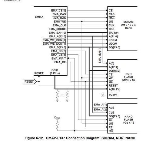
    Another thing that I am confused about is the address bus for the EMIFA.  On page 86 (picture below) of the OMAP-L137 data sheet there is an example configuration for the EMIFA with SDRAM, NOR, and NAND flash.  In order to increase the address bus size for the NOR flash it looks like they have hooked up 6 GPIO pins.  I haven’t been able to find anywhere that discusses how to configure this so that the controller knows about these pins.  Is that possible?  Or do you have to manually configure these, and manage the write cycles to the memory?  This also confuses me because the OMAP L137 Memory map for the asynchronous memorys specifies an available memory space of 32Mbit.  To me based on this memory map you would need at least 21 bit bus width in order to fill it so I was wondering if there was something I was missing about how to configure this for larger memory spaces. 

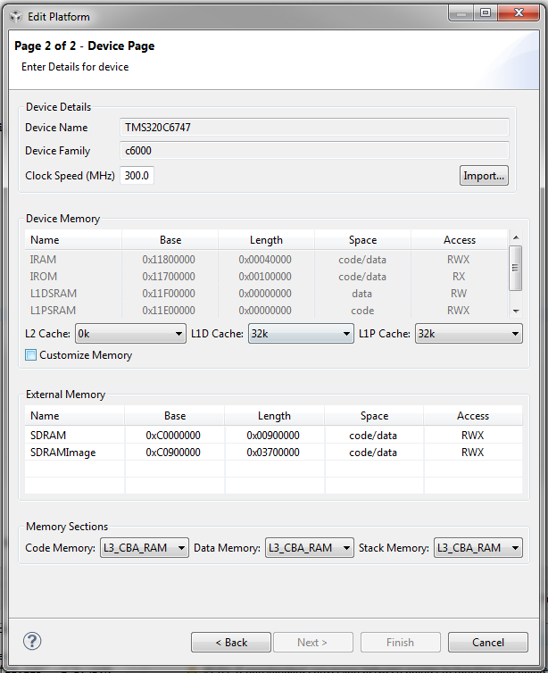
    Finally, for the OMAP-L137 dev kit I have been able to develop a secondary boot loader that allows me to flash the OMAP l137 from a terminal window after initial programming.  With that said I have a couple of questions about how the memory spaces will all work out for this.  In CCS in the Tool- RTCS Tools -> View/Edit Platform I pull up the memory mapping.   

    I want the boot loader to run entirely out of internal memory so I have setup everything to run out of the L2 Cache memory space and as a result I have it setup as follows below.  In this config I believe I have left L1D cache open and L1P cache open for the processor to actually use as cache, is that a correct assumption? 

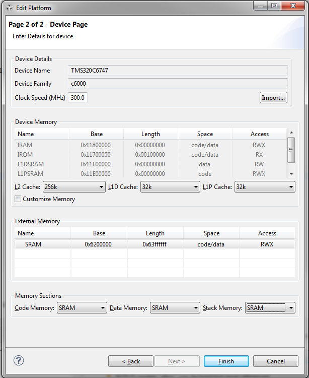
    When I compile and configure my run-time program I want it to run entirely out of the SRAM and leave as much of the CACHE available for CACHING in order to help mitigate some of speed degradation we will get due to using SRAM.  For this I plan to configure the memory space in the project as such:

    Is there anything I need to do when my secondary boot loader finishes running out of the L2 Cache and jumps to the main program in SRAM to designate that I want the SRAM to now be used as actual RAM instead of just a memory space for the bootloader program?


    I know there are a lot of questions here and I appreciate you support up front.


    Thanks,

    Chris


  • Hi Chris,
    Thanks for your detailed explanations.


    It is my understanding that the *.cmd file is generated by the AISGen tool when combining the boot configuration, and the .out file we want to flash to the tool. How do I modify this? I haven't been able to find any documentation specifying where I would find a custom file, what the format is, or how to modify it to configure the registers that would be necessary for the SRAM.


    No, *.cmd file is required to generate *.out with each and every section declared.

    AISgen tool is to convert to *.out to *.ais file for booting image alone. If we want to boot the board with bootloader and application then we have to convert bootloader's *.out to *.ais file and application needs to be converted from *.out to *.bin.

    Please refer to the following TI wikis.

    processors.wiki.ti.com/.../Linker_Command_File_Primer
    processors.wiki.ti.com/.../Linker_CMD_Files_for_CCS


    It is my understanding that the *.cmd file is generated by the AISGen tool when combining the boot configuration, and the .out file we want to flash to the tool. How do I modify this? I haven't been able to find any documentation specifying where I would find a custom file, what the format is, or how to modify it to configure the registers that would be necessary for the SRAM.


    As far I know, we can use GPIO pins for NOR flash higher address lines, we have to configure it through software and NOR is XIP so, we may need to change some software part for that to access the GPIOs as address lines.

    I will get back to you on this to provide more input.


    I want the boot loader to run entirely out of internal memory so I have setup everything to run out of the L2 Cache memory space and as a result I have it setup as follows below. In this config I believe I have left L1D cache open and L1P cache open for the processor to actually use as cache, is that a correct assumption?

    Yes, you are assumption was correct.


    Is there anything I need to do when my secondary boot loader finishes running out of the L2 Cache and jumps to the main program in SRAM to designate that I want the SRAM to now be used as actual RAM instead of just a memory space for the bootloader program?

    We need to get the "entry point" of main program from that project's *.map file and need use it in bootloader code to jump.
  • Thank you for the extra resources on the .cmd files.  I think that has helped me get a better understanding of that and how it maps the different memory sections.  The thing that I am still confused about is how this defines whether the sections for the L1D RAM and L1P RAM etc are going to be defined as being used as cache.  Is it simply if they are missing from this linker file that they will be defined and used as Cache for the system?  

    Also I didn't seem to catch the answer to my question about the secondary program from the bootloader.  How does the memory map from the Bootloader.cmd file influence the AppProgram.cmd file setup?  Are they completely independent so that once I have jumped to the AppProgram from my bootloader it will abide by the AppProgram.cmd memory configuraiton, including the caching setup?  What I want is that even though I will use some of the itnernal memory for the bootlaoder, I want all of it available for the AppProgram to be used as cache after the jump has been made.  

    I am not sure if I am following how we would "modify" SW in order to use extended address lines for the NOR Flash.  If htis is where the program resides I assume that things such as op code fetches and stuff have to be happening a very low level of the processor based on cache hits, misses, etc.  Seems like this would have to be a HW configuration unless I am missing how the whole system goes together.  

    Thanks,

    Chris

  • Hi Chris,

    Apologize for the delay in response.


    The thing that I am still confused about is how this defines whether the sections for the L1D RAM and L1P RAM etc are going to be defined as being used as cache. Is it simply if they are missing from this linker file that they will be defined and used as Cache for the system?

    Yes, if you missed to declare then it would take default configuration as cache for L1 (Program and Data).
    Please refer to the OMAPL138 TRM, chapter 5.3 "DSP Memories"


    Also I didn't seem to catch the answer to my question about the secondary program from the bootloader. How does the memory map from the Bootloader.cmd file influence the AppProgram.cmd file setup? Are they completely independent so that once I have jumped to the AppProgram from my bootloader it will abide by the AppProgram.cmd memory configuraiton, including the caching setup? What I want is that even though I will use some of the itnernal memory for the bootlaoder, I want all of it available for the AppProgram to be used as cache after the jump has been made.


    I would like to suggest to use L3 RAM/Shared RAM (128KiB) for bootloader code and DDR for application code with L1/L2 cached.

    What do you say ? Please share your thoughts on this.

    You have to use bootloader code for ARM only since it is OMAPL138, ARM is the master which comes out of reset first and wakeup the DSP next.

    Edited:

    You are using OMAPL137, here DSP is the master which comes out of reset first and wakeup the ARM next.

    So, you have to use bootloader for DSP and application could be anything, ARM or DSP.


    How about the application code ?
    Is that ARM executable or DSP executable ?
    Its already implemented and tested, refer OMAPL138 starterware and flashing TI wiki page.

    processors.wiki.ti.com/.../OMAPL138_StarterWare_Booting_And_Flashing


    I am not sure if I am following how we would "modify" SW in order to use extended address lines for the NOR Flash. If htis is where the program resides I assume that things such as op code fetches and stuff have to be happening a very low level of the processor based on cache hits, misses, etc. Seems like this would have to be a HW configuration unless I am missing how the whole system goes together.

    I'm discussing with hw team for this. Thanks for patience.
    In my understanding, I won't find any registers to access the GPIO as address line or conveying to EMIFA controller to act GPIO as address line.
    FYI: Already I have used one GPIO line for higher address lines on NOR flash. Just I have written software to assert that GPIO when I accessed that higher address space.