This thread has been locked.

If you have a related question, please click the "Ask a related question" button in the top right corner. The newly created question will be automatically linked to this question.

More Gel Script Problems with AM1705

Other Parts Discussed in Thread: AM1707, AM1705, AM1808, OMAP-L137, OMAP-L138

Hi all,

After sorting out the previous problem with the Gel script I have been going though it and writing my own based on the AM1707 script. However when I run it, there are still problems. The device becomes unresponsive very similar to before but I've checked that I'm not writing anything to reserved bits this time. 

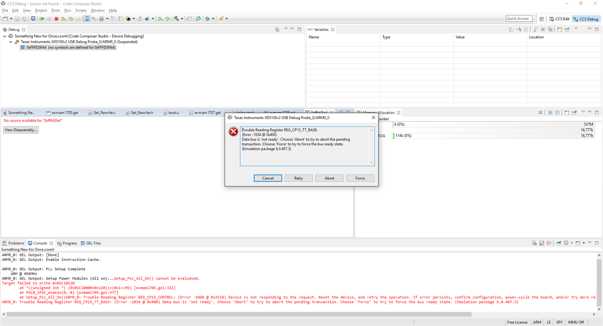
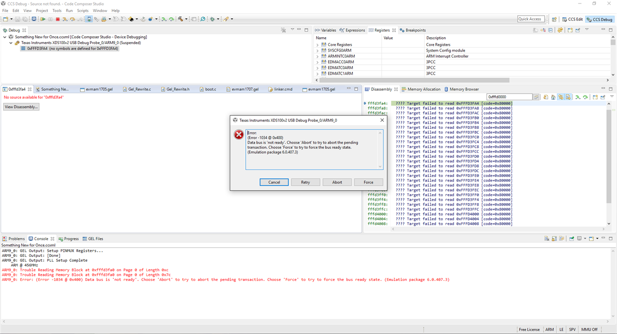
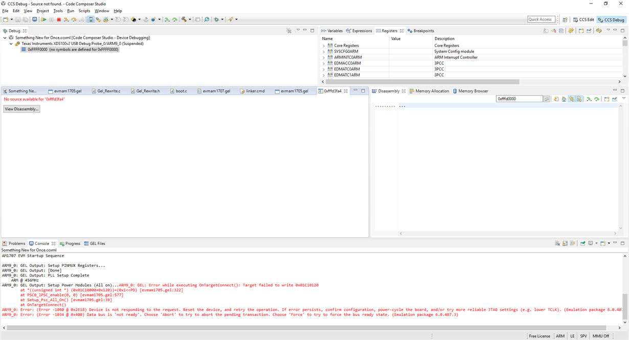
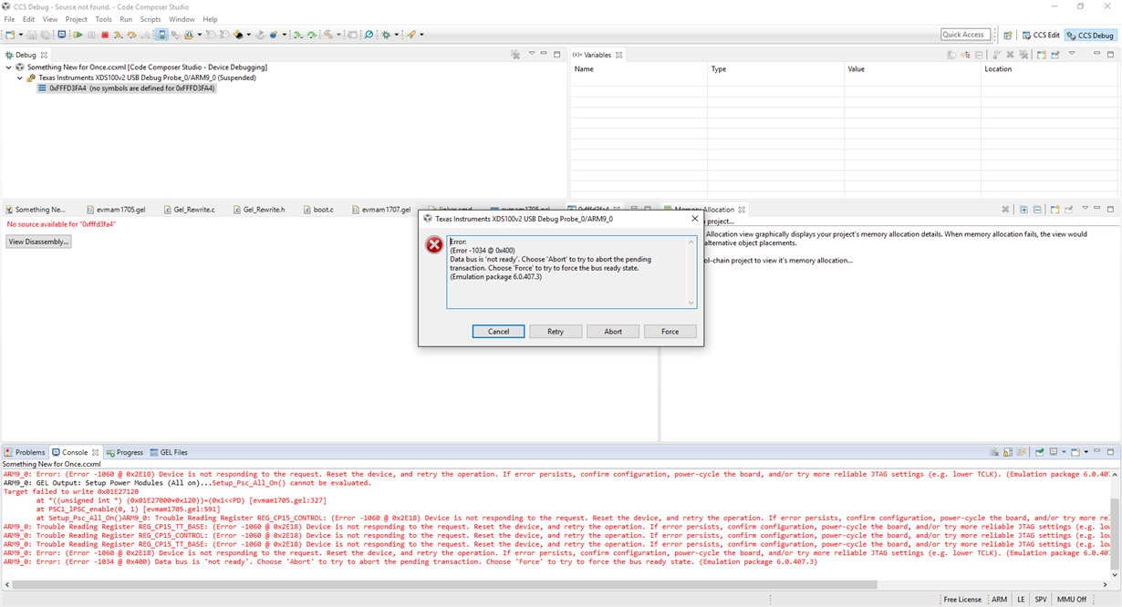
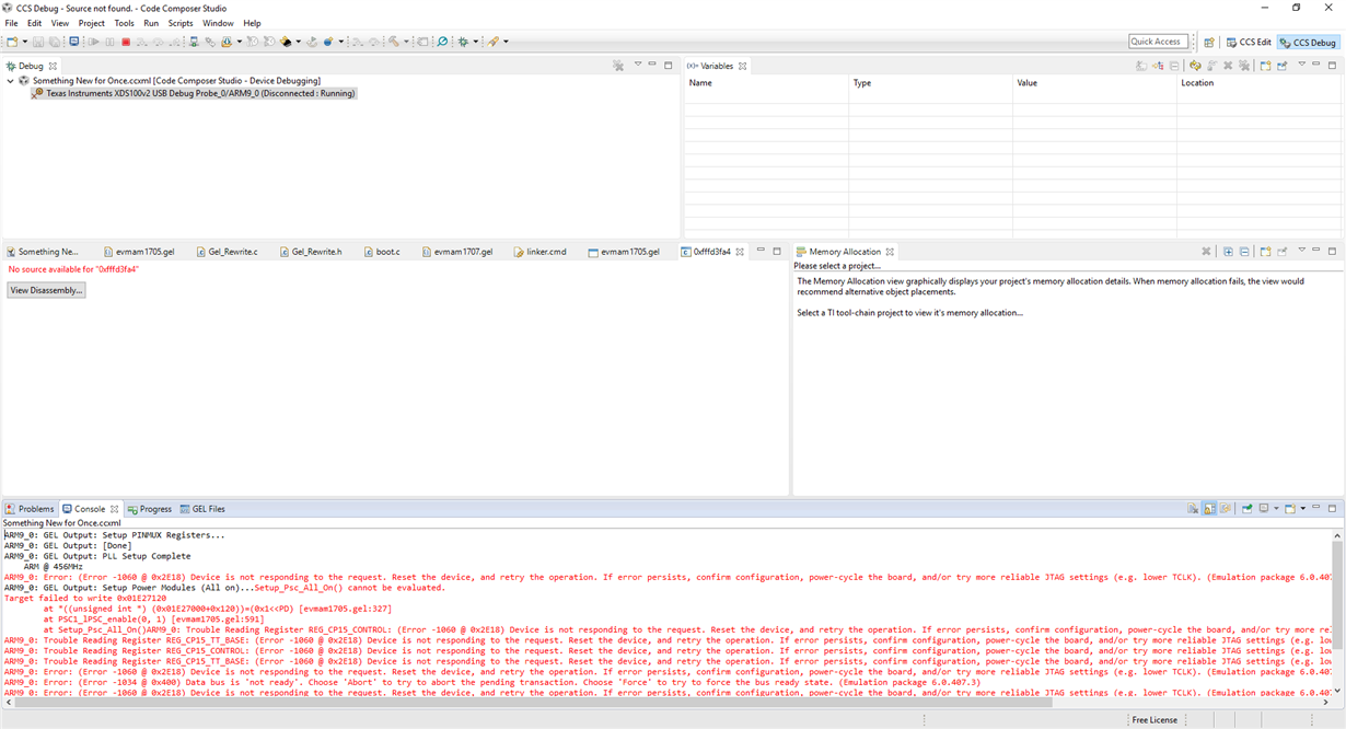
Here are the screenshots of the errors: 

I have also tried converting the Gel script to a C file and building it as part of the project with little success. What I have noticed however is that it seems to be halting at different time nearly every time I run it which is making it quite hard to debug. Any help will be greatly appreciated.

I've attache the Gel Script belowevmam1705.gel

  • This error is occurring while accessing the PTCMD register of PSC (for PSC0 EDMA3 CC0).

    Comment out the lines like below and try.
    // PSC0_lPSC_enable(0, 0);
    // PSC0_lPSC_enable(0, 1);
    // PSC0_lPSC_enable(0, 2);
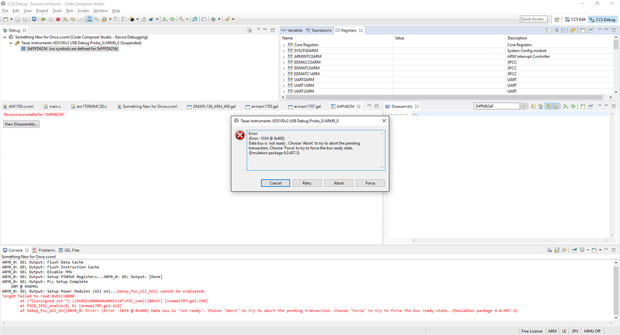
  • After commenting out all of the line for PSC0 I get the following:

    Also do I need to initialise those modules for the NANDWriter program to work correctly?

  • Can you please check the below post ?
    e2e.ti.com/.../1588722
    I've seen similar issue "cannot be evaluated" in CCSv6 for older gel scripts.

    Your issue seems to be same like "cannot be evaluated" in CCS.


    I have also tried converting the Gel script to a C file and building it as part of the project with little success. What I have noticed however is that it seems to be halting at different time nearly every time I run it which is making it quite hard to debug. Any help will be greatly appreciated.

    You said, that you were able to success by converting this gel to C code, sounds like CCS is the problem for running the gel script (executing the gel script)

    If its possible, try to run this gel in CCSv5.
  • My apologies when I said with little success I meant that it didn't work either. The processor hung at the PLL configuration and then when I reloaded it then hung during the PSC configuration.

    I'm going to install CCSv5 and see if that makes any difference. I'm also going to update to the latest CCSv6 as it seems to have some fixes for flashing devices.

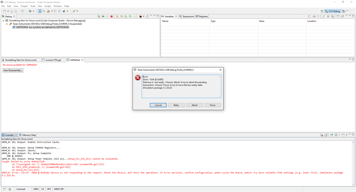
  • I have tried CCSv5.5 and I get the following error:

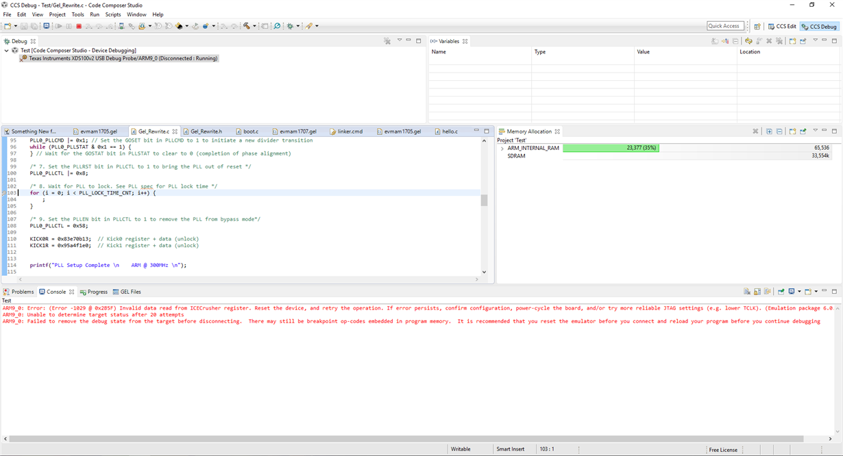
    and then when I've rewritten the GEL script into C code I get the following:

    I've also attached my C code: 

    Gel_Rewrite.c
    /*
     * Gel_Rewrite.c
     *
     *  Created on: 11 Sep 2016
     *      Author: Demon
     */
    
    #include "Gel_Rewrite.h"
    #include <stdio.h>
    
    int Gel_Rewrite(void) {
    
    	int i = 0;
    	/* Configure ARM at 300MHz, EMIFs at 100MHz */
    	unsigned int CLKMODE = 0;
    	unsigned int PLLM = 24;		// Multiplier of 25 to set PLL out = 600MHz
    	unsigned int POSTDIV = 1;		// Divider of 2 to set Clock Out = 300MHz
    	unsigned int PLLDIV3 = 2;		// Divider of 3 to set SYSCLOCK3 = 100MHz
    	unsigned int PLLDIV5 = 2;		// Divider of 3 to set SYSCLOCK3 = 100MHz
    	unsigned int PLLDIV7 = 5;		// Divider of 6 to set SYSCLOCK3 = 50MHz


    	printf("Setting up PINMUX Regs\n");
    
    	// 1. Set KICK Registers to magic values, see Datasheet
    	KICK0R = 0x83e70b13;
    	KICK1R = 0x95a4f1e0;
    
    
    	// Can write to SYSCON registers.
    	PINMUX0 = 0x11112100;  	// EMIFB and RTCK
    	PINMUX1 = 0x11111111;  	// EMIFB
    	PINMUX2 = 0x01111111;  	// EMIFB
    	PINMUX3 = 0x00000000;  	// Reserved
    	PINMUX4 = 0x00000000;  	// Reserved
    	PINMUX5 = 0x11111110;  	// EMIFB
    	PINMUX6 = 0x11111111;  	// EMIFB
    	PINMUX7 = 0x11111111; 	// EMIFB and SPI0
    	PINMUX8 = 0x20011100;  	// UART2, BOOT7 and UART0
    	PINMUX9 = 0x00000002;  	// UART2
    	PINMUX10 = 0x00000000;  // No Use
    	PINMUX11 = 0x00081188;  // UART1
    	PINMUX12 = 0x88808800;  // GPIO
    	PINMUX13 = 0x11088888;  // EMIFA
    	PINMUX14 = 0x00111111;  // EMIFA
    	PINMUX15 = 0x10000000;  // EMIFA
    	PINMUX16 = 0x00000001;  // EMIFA
    	PINMUX17 = 0x00011000;  // EMIFA
    	PINMUX18 = 0x00110010;  // EMIFA
    	PINMUX19 = 0x00000001;  // EMIFA
    
    	//  Force Device Operation, Clock Sourced Internally, 48MHz no-sleep mode, Comparators enabled, 24MHz USB Input Clock
    	CFGCHIP2 = 0x00004872;
    	CFGCHIP2 |= 0x00001000; // Enable USB0 clock
    
    	printf("[Done]\n");
    
    
    	// Setup_PLL()
    	printf("Setting up PLL\n");
    
    
    	/* 1. Put PLL in reset and select bypass mode  */
    	PLL0_PLLCTL &= 0xFFFFFFF6;          // PLLEN=0 (Bypass) and PLLRST=0 (reset)
    	for (i = 0; i < PLLEN_MUX_SWITCH; i++) {
    		;
    	}   // Wait for 4 OSCIN cycles to ensure proper trasition to bypass clock
    
    	/* 2. Select the Clock Mode bit 8 as External Clock or On Chip Oscilator */
    	PLL0_PLLCTL &= 0xFFFFFEFF;
    	PLL0_PLLCTL |= (CLKMODE << 8);  // Internal oscillator (crystal)
    	PLL0_PLLCTL &= 0xFFFFFFDF;   // Set PLLENSRC '0',bit 5 -> PLL Enable(PLLEN)
    
    	/* 3. Clear PLLRST bit to 0 -Reset the PLL */
    	PLL0_PLLCTL &= 0xFFFFFFF7;
    
    	/* 4. Clear the PLLPWRDN bit to bring the PLL out of power-down mode */
    	PLL0_PLLCTL &= 0xFFFFFFFD;
    
    	/* 5. Program the required multiplier value in PLLM and POSTDIV */
    	PLL0_PLLM = PLLM;              		// Multiplier value = PLLM + 1
    	PLL0_POSTDIV = 0x8000 | POSTDIV; 	// If desired to scale all the SYSCLK frequencies of a given PLLC
    
    	/* 6. program PLLDIVn registers to change the SYSCLK0 to SYSCLKn divide values */
    	while (PLL0_PLLSTAT & 0x1 == 1) {
    		;
    	} // Wait for GOSTAT bit in PLLSTAT to clear to indicate no GO operation is currently in progress
    
    	// Program the RATIO field in PLLDIVx with the desired divide factors. Make sure to leave the PLLDIVx.DxEN bits set so clocks are still enabled
    	PLL0_PLLDIV3 = 0x8000 | PLLDIV3; // SYSCLK3 -> EMIFA
    	PLL0_PLLDIV5 = 0x8000 | PLLDIV5; // SYSCLK5 -> EMIFB
    	PLL0_PLLDIV7 = 0x8000 | PLLDIV7; // SYSCLK7 -> EMAC/MDIO
    
    	PLL0_PLLCMD |= 0x1; // Set the GOSET bit in PLLCMD to 1 to initiate a new divider transition
    	while (PLL0_PLLSTAT & 0x1 == 1) {
    	} // Wait for the GOSTAT bit in PLLSTAT to clear to 0 (completion of phase alignment)
    
    	/* 7. Set the PLLRST bit in PLLCTL to 1 to bring the PLL out of reset */
    	PLL0_PLLCTL |= 0x8;
    
    	/* 8. Wait for PLL to lock. See PLL spec for PLL lock time */
    	for (i = 0; i < PLL_LOCK_TIME_CNT; i++) {
    		;
    	}
    
    	/* 9. Set the PLLEN bit in PLLCTL to 1 to remove the PLL from bypass mode*/
    	PLL0_PLLCTL = 0x58;
    
    	KICK0R = 0x83e70b13;  // Kick0 register + data (unlock)
    	KICK1R = 0x95a4f1e0;  // Kick1 register + data (unlock)
    
    
    	printf("PLL Setup Complete \n    ARM @ 300MHz \n");
    
    	printf("Setup Power Modules (All on)... ");
    
    	// PSC0
    
    	while ((PSC0_PTSTAT & 0x1)) {
    		;
    	}
    
    	// Set the modules to transition to enabled state
    	PSC0_MDCTL0 = 0x3;			// EDMA3 Channel Controller
    	// Initiate transition
    	PSC0_PTCMD |= 0x1;
    	// Check that it's complete or wait till it is.
    	while ((PSC0_PTSTAT & 0x1)) {
    		;
    	}
    
    	PSC0_MDCTL1 = 0x3;			// EDMA3 Transfer Controller 0
    
    	PSC0_PTCMD |= 0x1;
    	while ((PSC0_PTSTAT & 0x1)) {
    		;
    	}
    
    	PSC0_MDCTL2 = 0x3;			// EDMA3 Transfer Controller 1
    
    	PSC0_PTCMD |= 0x1;
    	while ((PSC0_PTSTAT & 0x1)) {
    		;
    	}
    
    	PSC0_MDCTL3 = 0x3;			// EMIFA
    
    	PSC0_PTCMD |= 0x1;
    	while ((PSC0_PTSTAT & 0x1)) {
    		;
    	}
    
    	PSC0_MDCTL4 = 0x3;			// SPI0
    
    	PSC0_PTCMD |= 0x1;
    	while ((PSC0_PTSTAT & 0x1)) {
    		;
    	}
    
    	PSC0_MDCTL9 = 0x3;			// UART0
    
    	PSC0_PTCMD |= 0x1;
    	while ((PSC0_PTSTAT & 0x1)) {
    		;
    	}
    
    	PSC0_MDCTL14 = 0x3;			// ARM
    
    	PSC0_PTCMD |= 0x1;
    	while ((PSC0_PTSTAT & 0x1)) {
    		;
    	}
    
    	printf("PSC0 setup complete\n");
    
    
    	PSC1_MDCTL1 = 0x3;			// USB0
    
    	PSC1_PTCMD |= 0x1;
    	while ((PSC1_PTSTAT & 0x1)) {
    		;
    	}
    
    	PSC1_MDCTL3 = 0x3;			// GPIO
    
    	PSC1_PTCMD |= 0x1;
    	while ((PSC1_PTSTAT & 0x1)) {
    		;
    	}
    
    	PSC1_MDCTL6 = 0x3;			// EMIFB
    
    	PSC1_PTCMD |= 0x1;
    	while ((PSC1_PTSTAT & 0x1)) {
    		;
    	}
    
    	PSC1_MDCTL12 = 0x3;			// UART1
    
    	PSC1_PTCMD |= 0x1;
    	while ((PSC1_PTSTAT & 0x1)) {
    		;
    	}
    
    	PSC1_MDCTL13 = 0x3;			// UART2
    
    	PSC1_PTCMD |= 0x1;
    	while ((PSC1_PTSTAT & 0x1)) {
    		;
    	}
    
    	printf("PSC1 setup complete\n");
    
    	// NAND Flash Setup
    
    	/* Use extended wait cycles to keep CE low during NAND access */
    	AEMIF_AWCCR = 0xff;
    
    	/* Setup CS3 - 8-bit NAND */
    	AEMIF_A2CR = 0x00300388;
    	AEMIF_NANDFCR |= 2;


    	return 0;
    }


    Gel_Rewrite.h

  • The above error occurs during printf("Setup Power Modules (All on)... "); After commenting out this line then it runs till I try and setup PSC0_MDCTL3 =0x3. This causes the same error to occur.
  • I assumed you started with a working evmam1707.gel file and then made changes for the AM1705. Maybe try rolling back your changes one by one until things start to work.

    Maybe add back the call to Disable_IRQ_Flush_Cache() and all the contents of Disable_IRQ_Flush_Cache(). The function seems to do more than disable IRQ. It apparently puts the processor is supervisor mode and disables the MMU. I think both of those are needed. The KICK unlock is commented out as well. In theory, out of reset, the KICK should already be unlocked. Unless KICK has been disabled like in later 6748 versions. Then don't bother.
  • I started with the AM1707 gel script from Spectruum Digital, support.spectrumdigital.com/.../evmam1707.gel which doesn't have the Disable_IRQ_Flush_Cache() function at all. But I've found a gel script for either the AM1808, OMAP137 or OMAP138 that has it and I'll have a look at that and include it.

    Yes the KICK registers have been commented out at the end of the PLL setup as they were causing the program to hang which I thought was quite bizarre. The registers are written to at the start of the Setup_System_Config() call and I always run that one first to ensure that they are unlocked.
  • I compared your GEL to the one posted here:
      e2e.ti.com/.../151682
      sw_am17x.zip
    See attached file.

    evmam1707.gel

    Did you check your CCS install directory for an EVMAM1707.GEL file? My very old CCS 5 does not have one. I would expect the newest CCS to support the EVM with an appropriate GEL script file.

  • I've tried your file and the one that comes with the installation (1777.evmam1707.gel)

    and I'm still getting errors. I've had to change the PINMUX registers and some of the PLL configs as my AM1705 is configured for 375MHz. I also tried it with both of the scripts:

    Test 1: AM17xx Starterware Gel

    Change the PINMUX registers to match my previous script and the PLL config to match my previous script. The following error was observed: 

    Test 2: CCS Gel Script

    I change the PINMUX registers to be all set to GPIO and the PLLM variable to be 15 for a clock of 360MHz. The following error was observed:

    The errors are the same regardless of if the OnTargetConnect() function is called or if I manually run through them using the scripts menu. What is interesting is that they seem to occur at different times. Using Test 1's Gel and stepping through the functions I found that changing the KICK1 register in the PLL setup was causing the error however when running through it with the Target Connect call then it ran to point as shown in the screenshot. 

  • A bit of a summary...

    1) PLLM=24
    Setup PINMUX
    PLL Setup
    Setup Power Modules - fails on first access to PSC0

    2) PLLM=24
    Setup PINMUX
    PLL Setup
    Setup Power Modules - comment out PSC0, fails on first access to PSC1

    3) PLLM=24?
    Flush Data Cache
    FLush Instruction Cache
    Disable MMU
    Setup PINMUX
    PLL Setup
    Setup Power Modules- fails on first access to PSC0

    4) PLLM=15
    Flush Data Cache
    FLush Instruction Cache
    Disable MMU
    Setup PINMUX
    PLL Setup - fails on PLLCTL enable

    From what I can see, in the first 3 scenarios, the processor has hung after PLL setup. It implied that PLL has not locked and the processor clock is unstable. I am guessing scenario 4 fails on the script line that enables the PLL clock to the processor. Seems slower speed results in immediate fail. You could try commenting out that line only:
    PLL0_PLLCTL |= 0x1;
    Your GEL script should complete but the processsor will by running at a really slow clock. Peripherals like the UART won't be happy. Perhaps get your HW guys to check all the PLL components.
  • Your summary is correct.
    I'll try commenting out the final line in the PLL setup.
    Could you let me know what I should look for with regards to the PLL components? I'm the hardware and software guy on this project. I'm guessing check the crystal is oscillating correctly and that the power supply is stable?
  • Unfortunately, I'm a firmware guy. I would not know but the things you are saying sounds a lot like the stuff I hear from my HW guy. The AM1705 datasheet SPRS657D has some design considerations in 5.6 Crystal Oscillator or External Clock Input, and 5.7 Clock PLLs sections. Those sections mention some capacitors and ferrite beads. I suppose you could setup the OBSCLK pin to see a divided down version of the PLL output.

    Hopefully some HW guys will speak up.
  • Ok, thanks for all the help Norman. I'll let you know what I find out
  • So I've checked the power supply for the PLL and as well as the XOUT. Both look good at boot and then when I run the Gel Script the XOUT waveform disappears and is replaced by a 0.8V DC voltage. I also noticed that the XGND is at a higher potential then DGND by about 0.2V.
    Any advice from the Hardware Guys on the forums?
  • Dear Haydn,
    I requested HW team to look into this issue.
    You would get response soon.
    Thanks for your patience.
  • Sorta sounds like the clock mode went from crystal/internal to external clock.

    Some oddness in the GEL scripts.

    Bit 9 (EXTCLKSRC) of PLLCTL is reserved on the OMAP-L137 and derivatives, AM1705, AM1707, C6747, etc. This line probably should be removed
    PLL0_PLLCTL &= 0xFFFFFDFF; // PLLCTL.EXTCLKSRC bit 9 should be left at 0
    I think you already removed it from your C code. Setting bit 9 to 0 is in pretty well all the GEL scripts and it hasn't seem to be problem yet.

    The first line of the PLL config is slightly different in some GEL scripts
    PLL0_PLLCTL &= 0xFFFFFFF6; // PLLEN=0 (Bypass) and PLLRST=0 (reset)
    is sometimes like this
    PLL0_PLLCTL &= 0xFFFFFFFE; // PLLEN=0 (Bypass)
    The PLLRST is asserted later in the process. Maybe the PLL has to be out of reset to do the bypass.

    The OMAP-L138 GEL scripts ensure CFGCHIP0.PLL_MASTER_LOCK is cleared but it should already be cleared on POR.
  • That's what I thought as well but I have checked the script and it definitely set the clock mode to 0 for crystal.
    I have also thought about that line but since it doesn't change anything I didn't think it would matter (set to 0 on POR)
    I'll look into the Bypass and Reset aspect of it although again it isn't changing anything as it is set that way after POR.
    I tried changing my load capacitors as I thought that they could be a bit low but that ended up killing my waveform even on POR so I'm going to change them back later today and I'll try the Bypass only line in the Gel script
  • Yeah, you are right that the POR defaults match whatever the GEL script wants to change them to. HW is looking suspicious. Are you using a current limiting power supply? I sometimes get caught setting it too low when I bring up an custom design for the first time.
  • No I'm not. I kinda thinking that I may try do the bare minimum to take the PLL out of reset seeing as it defaults to a 20x multiplier and /2 postdiv. It also defaults to using the crystal so if that works then I know for sure that it is something that I'm initialising incorrectly

  • I've managed to find these threads who seem to be having a similar issue:

    e2e.ti.com/.../713387

    e2e.ti.com/.../289397

    I checked the resistance between XGND and VSS and it was 20ohms when the device is unpowered and 0ohms when it is powered. This is correct?
    I was also wondering if any one heard anything further from the second thread?
  • It seems that I've managed to solve the PLL initialisation problem. I tried changing the loading capacitors and that completely destroyed the signal so I replaced them and I applied more heat to the ground pad as per one of the threads before. I can now complete the PLL initialisation without a problem whether I step through it or not. However I've come across another problem, it seems the voltage is dropping too low when I enable the EMIFA in the PSC initialisation however I probed the 1.2V rail and there was no change there so could it be on the 3.3V rail?
  • Seems to be no other takers. Thinking aloud here. When you say "the voltage is dropping too low", what voltage is that? The 3.3V rail should be for the I/O pins only. Powering up and clocking the EMIFA should not result in any I/O pins going active. Just the EMIFA controller drawing from clock modules SYSCLK3 and that should be at 1.2V. No idea which pin is powering the clock module. Maybe check the voltage at pins PLL0_VDDA and CVDD (all 16 of them). Preferably on top on the pin and not at the PCB pad.
  • I'm not too sure which rail it is. The error from the debugger is that "the Target has experienced a power loss.". If it's only the 1.2V rail that needs probing then that is great as it limits what I have to probe. I've already checked the power on the PLL0_VDDA and that is stable throughout the initialisation phase.
  • In theory, the debugger can only see what JTAG is connected to. The JTAG pins are 3.3V logic. There are 22 of those DVDD pins! Can't think of mechanism that link EMIFA power/clock to JTAG going down. Maybe powering up and clocking EMIFA does take some of the EMIFA lines out of hi-Z. Possibly those EMIFA lines are shorted to the JTAG pins somewhere. I would expect EMIFA pins to stay hi-Z until EMIFA is actually configured and actively being accessed.
  • I can definitely confirm that the JTAG lines aren't connected on the board except where they need to be. I guess what is needed right is someone from hardware to give me some direction because at the moment I'm just taking random stabs in the dark.
    I'm going to change my power inductors as they are a little on the big side. Maybe add some more capacitance if I can?
  • I think the TI guys probably assume that I keeping the debug process going. You might need to start a new thread. I'm out of ideas. Maybe try replying to Titusrathinaraj Stalin last post. That might bump this thread.
  • Hello Haydn,

    I want you to first check all the power rails, reset and clocks are stable ?

    Are you able to connect to the target now ? or still getting "Target has experienced a power loss" error ?

    Regards,
    Senthil
  • It seems that I managed to solve this error by increasing the current limit on my power supply to 1A. It was previously at 500mA and the board was drawing about 25mA so I didn't really think it could be the power supply. But that's all I've changed.

    In summary for anyone who else finds this thread, the PLL and PSC error was solved by heating up the ground pad again to make sure that it was soldered correctly and then the next error was caused by a current limit that was too low.

    Thanks for all the help everybody but especially Norman!
  • Nevermind. I see that I forgot to uncomment the line of code causing the error but I think I'll start a new thread for this.

    I'll also let you know that when I include the line of code that sets the clock mode then my core hangs and I get the error however when I use everything else and leave those lines commented out then the GEL Script runs to completion. I've attached my current GEL Script if you're interested.8080.evmam1705.gel

  • Well, I'll state the obvious with CLKMODE script lines:
    //PLL0_PLLCTL &= 0xFFFFFEFF;
    //PLL0_PLLCTL |= (CLKMODE<<8); // Internal oscillator (crystal)
    PLL0_PLLCTL &= 0xFFFFFFDF; // Set PLLENSRC '0',bit 5 -> PLL Enable(PLLEN)
    The lines have not effect as the CLKMODE bit should be already 0. Unless writing 0 to CLKMODE that is already 0 triggers something in the processor. Try dumping out the PLLCTL value at various points, eg.

    GEL_TextOut( "0.PLL0_PLLCTL = %x\n", 0, 0, 0, 0, PLL0_PLLCTL );

    /* 1. Put PLL in reset and select bypass mode */
    PLL0_PLLCTL &= 0xFFFFFFF6; // PLLEN=0 (Bypass) and PLLRST=0 (reset)
    for (i = 0; i < PLLEN_MUX_SWITCH; i++) {
    ;
    } // Wait for 4 OSCIN cycles to ensure proper trasition to bypass clock

    GEL_TextOut( "1. PLL0_PLLCTL = %x\n", 0, 0, 0, 0, PLL0_PLLCTL );

    /* 2. Select the Clock Mode bit 8 as External Clock or On Chip Oscilator */
    //PLL0_PLLCTL &= 0xFFFFFEFF;
    //PLL0_PLLCTL |= (CLKMODE<<8); // Internal oscillator (crystal)
    PLL0_PLLCTL &= 0xFFFFFFDF; // Set PLLENSRC '0',bit 5 -> PLL Enable(PLLEN)

    GEL_TextOut( "3. PLL0_PLLCTL = %x\n", 0, 0, 0, 0, PLL0_PLLCTL );
  • This is the output when the CLKMODE lines are still commented out:

    CLKMODE commented out.txt
    ARM9_0: GEL Output: Setup PINMUX Registers...ARM9_0: GEL Output: [Done]
    ARM9_0: GEL Output: 0.PLL0_PLLCTL = 0x00000072
    ARM9_0: GEL Output: 1.PLL0_PLLCTL = 0x00000072
    ARM9_0: GEL Output: 2.PLL0_PLLCTL = 0x00000052
    ARM9_0: GEL Output: 3.PLL0_PLLCTL = 0x00000052
    ARM9_0: GEL Output: 4.PLL0_PLLCTL = 0x00000050
    ARM9_0: GEL Output: 5.PLL0_PLLCTL = 0x00000050
    ARM9_0: GEL Output: 6.PLL0_PLLCTL = 0x00000050
    ARM9_0: GEL Output: 7.PLL0_PLLCTL = 0x00000058
    ARM9_0: GEL Output: 8.PLL0_PLLCTL = 0x00000058
    ARM9_0: GEL Output: 9.PLL0_PLLCTL = 0x00000000
    ARM9_0: GEL Output: PLL Setup Complete 
    ARM @ 300MHz 
    ARM9_0: Trouble Reading Memory Block at 0xfffd3fa0 on Page 0 of Length 0xc 
    ARM9_0: Trouble Reading Memory Block at 0xfffd3fa0 on Page 0 of Length 0x90 
    ARM9_0: Error: (Error -1034 @ 0x400) Data bus is 'not ready'. Choose 'Abort' to try to abort the pending transaction. Choose 'Force' to try to force the bus ready state. (Emulation package 6.0.407.6) 
    ARM9_0: Error: (Error -1035 @ 0x2EE0) Device state appears corrupt after a hung bus. Power-cycle the board. If error persists, confirm configuration and/or try more reliable JTAG settings (e.g. lower TCLK). (Emulation package 6.0.407.6) 
    ARM9_0: Error: (Error -1034 @ 0x400) Data bus is 'not ready'. Choose 'Abort' to try to abort the pending transaction. Choose 'Force' to try to force the bus ready state. (Emulation package 6.0.407.6) 
    ARM9_0: Error: (Error -1035 @ 0x2EE0) Device state appears corrupt after a hung bus. Power-cycle the board. If error persists, confirm configuration and/or try more reliable JTAG settings (e.g. lower TCLK). (Emulation package 6.0.407.6)

    and this is with it enabled:

    CLKMODE Enabled.txt
    ARM9_0: GEL Output: Disable IRQ/FIQ
    ARM9_0: GEL Output: Flush Data Cache
    ARM9_0: GEL Output: Flush Instruction Cache
    ARM9_0: GEL Output: Disable MMU
    ARM9_0: GEL Output: Setup PINMUX Registers...ARM9_0: GEL Output: [Done]
    ARM9_0: GEL Output: 0.PLL0_PLLCTL = 0x00000072
    ARM9_0: GEL Output: 1.PLL0_PLLCTL = 0x00000072
    ARM9_0: GEL Output: 2.PLL0_PLLCTL = 0x00000052
    ARM9_0: GEL Output: 3.PLL0_PLLCTL = 0x00000052
    ARM9_0: GEL Output: 4.PLL0_PLLCTL = 0x00000050
    ARM9_0: GEL Output: 5.PLL0_PLLCTL = 0x00000050
    ARM9_0: GEL Output: 6.PLL0_PLLCTL = 0x00000050
    ARM9_0: GEL Output: 7.PLL0_PLLCTL = 0x00000058
    ARM9_0: GEL Output: 8.PLL0_PLLCTL = 0x00000058
    ARM9_0: GEL Output: 9.PLL0_PLLCTL = 0x0000005D
    ARM9_0: GEL Output: PLL Setup Complete 
        ARM @ 300MHz 
    ARM9_0: Trouble Reading Memory Block at 0xfffd3fa0 on Page 0 of Length 0xc 
    ARM9_0: Trouble Reading Memory Block at 0xfffd3fa0 on Page 0 of Length 0x60 
    ARM9_0: Error: (Error -1034 @ 0x400) Data bus is 'not ready'. Choose 'Abort' to try to abort the pending transaction. Choose 'Force' to try to force the bus ready state. (Emulation package 6.0.407.6) 
    ARM9_0: Error: (Error -1035 @ 0x2EE0) Device state appears corrupt after a hung bus. Power-cycle the board. If error persists, confirm configuration and/or try more reliable JTAG settings (e.g. lower TCLK). (Emulation package 6.0.407.6) 
    

  • Looking at the PLLCTL values, the "Enabled" case looks better. The "Commented Out" case is the same until the end where PLLCTL = 0. In both cases, the GEL script does not run to completion. Weird stuff is that reserved bits PLLCTL are not what they documented to be in the TRM and change during the PLL init.

    The next line "Setup Power Modules (All on)... " never appears. The debug output says it can't read 0xfffd3fa0, which according to the datasheet is ARM local ROM. Probably the boot ROM code. No idea why boot ROM is involved. It should have finished running assuming your boot mode pins are strapped for emulation boot. You should double check that.

    The printing changes the timing, that may be why both cases fail now. A real puzzle.
  • I checked the BOOTCFG register and that is set to the right values for emulation boot. I was previously running it by right clicking on target configuration and selecting launch configuration and so it didn't have a program loaded in. I think the emulation boot mode just causes it to loop back to a single instruction which is stored in the ROM. This is what I'm getting from the disassembly.

    Following this line of thought I tried to run the gel script once a program is loaded into its memory and it's waiting at the main() call (note: I've included a boot.c and set the linker to call that first. The boot.c code is based on the AM1707 User Bootloader that comes with the SDK.). When the GEL is run from there I get the following:

    Running with Program set to main().txt
    ARM9_0: GEL Output: 
    AM1707 EVM Startup Sequence
    
    ARM9_0: GEL Output: Disable IRQ/FIQ
    ARM9_0: GEL Output: Flush Data Cache
    ARM9_0: GEL Output: Flush Instruction Cache
    ARM9_0: GEL Output: Disable MMU
    ARM9_0: GEL Output: Setup PINMUX Registers...ARM9_0: GEL Output: [Done]
    ARM9_0: GEL Output: 0.PLL0_PLLCTL = 0x00000072
    ARM9_0: GEL Output: 1.PLL0_PLLCTL = 0x00000072
    ARM9_0: GEL Output: 2.PLL0_PLLCTL = 0x00000072
    ARM9_0: GEL Output: 3.PLL0_PLLCTL = 0x00000072
    ARM9_0: GEL Output: 4.PLL0_PLLCTL = 0x00000070
    ARM9_0: GEL Output: 5.PLL0_PLLCTL = 0x00000070
    ARM9_0: GEL Output: 6.PLL0_PLLCTL = 0x00000070
    ARM9_0: GEL Output: 7.PLL0_PLLCTL = 0x00000078
    ARM9_0: GEL Output: 8.PLL0_PLLCTL = 0x00000078
    ARM9_0: GEL Output: 9.PLL0_PLLCTL = 0x00000079
    ARM9_0: GEL Output: PLL Setup Complete 
        ARM @ 300MHz 
    ARM9_0: GEL Output: Setup Power Modules (All on)...ARM9_0: Trouble Writing Memory Block at 0x1c10120 on Page 0 of Length 0x4 
    ARM9_0: GEL: Error while executing OnTargetConnect(): Target failed to write 0x01C10120
    	at *((unsigned int *) (0x01C10000+0x120))=(0x1<<PD) [evmam1705.gel:324]
    	at PSC0_lPSC_enable(0, 3) [evmam1705.gel:614]
    	at Setup_Psc_All_On() [evmam1705.gel:41]
    	at OnTargetConnect()
    ARM9_0: Trouble Reading Register REG_ENDIAN: (Error -150 @ 0x2A3C) One of the FTDI driver functions used during configuration returned a invalid status or an error. (Emulation package 6.0.407.6) 
    ARM9_0: Trouble Reading Register REG_SYSTEM_TARGET_PSR: (Error -150 @ 0x2A3C) One of the FTDI driver functions used during configuration returned a invalid status or an error. (Emulation package 6.0.407.6) 
    ARM9_0: Trouble Reading Register REG_SYSTEM_TARGET_CONFIG: (Error -150 @ 0x2A3C) One of the FTDI driver functions used during configuration returned a invalid status or an error. (Emulation package 6.0.407.6) 
    ICEPICK_C: Error: (Error -150 @ 0x0) One of the FTDI driver functions used during configuration returned a invalid status or an error. (Emulation package 6.0.407.6) 
    ARM9_0: Trouble Reading Register REG_SYSTEM_MMU_CONFIG: (Error -150 @ 0x2A3C) One of the FTDI driver functions used during configuration returned a invalid status or an error. (Emulation package 6.0.407.6) 
    ARM9_0: Error: Failed to get PRSC status
    ARM9_0: Unable to determine target status after 20 attempts
    ARM9_0: Failed to remove the debug state from the target before disconnecting.  There may still be breakpoint op-codes embedded in program memory.  It is recommended that you reset the emulator before you connect and reload your program before you continue debugging
    

    Now when I try to use the right click for launch configuration I get the exact same output. 

    Final Note: I have uncommented the // PSC0_lPSC_enable(0, 3);  // EMIFA line.

    When this is commented out then the GEL script runs to completion.

  • In that output, PLLENSRC stays 1. It should be 0 but maybe PLLENSRC automatically goes back to 1 when a PLLRST assert is complete. Previous outputs have PLLENSRC remaining at 0. Not sure if that is a clue.

    I remember emulation boot is described in documentation as an infinite NOP loop located in ROM. When the debugger has "halted" the processor, nothing should be running. What is odd is that the debugger seems to "let go" and the processor seems to start running that infinite loop.

    So...the current GEL script runs to completion with
    - CLKMODE enabled
    - GEL_TextOut added
    - PSC EMIF is commented out

    Seemingly random behaviour seems to suggest a bad board. I know you said a while back that an another board is not avaiable. It that still the case?
  • Another test would be to not mux the EMIFA pins but still powerup/clock EMIFA. Leave them as tri-state. If the script completes, it would suggest that one of the EMIFA pins is shorted to something that would cause the hang. If the script does not complete, something might be happening internal to the processor.
  • I think in that run I had commented out PLLENSRC to be 0 and so the PLLEN bit has no effect and it runs to completion.
    I've tried removing the EMIFA PINMUX setup however it still hangs on the PLL0_PLLCTL |= 0x1; line.

    Unfortunately this design is for a university project and we're already over budget so I'm not going to get the opportunity to make another board. I'd like to work on it over the holidays however I'll have to discuss that with my supervisors.
  • Just in case anyone is still following this. I've made another board using an oscillator rather than a crystal and I'm experiencing the same issue. I'm in the process of trying to change the only thing common to both boards which is the JTAG programmer and I'll post something here if it works. Otherwise assume it didn't work