This thread has been locked.

If you have a related question, please click the "Ask a related question" button in the top right corner. The newly created question will be automatically linked to this question.

SPI0 slave unable to run continuously clocked 16-bit words @ 24MHz+ clock rate

Hello, 

I had a previous ticket where originally it was thought that the some lost words from the SPI peripheral was down to EDMA3 transfer issues (see post here ), but it turns out that the SPI peripheral is flagging issues on the SPI bus and are discarding words due to either bit length errors on SIMO or TX errors on SOMI (both very occasionally, say once every hour). We are running a single master and single slave (OMAP) SPI bus. The PCB line lengths for CS, SOMI, SIMO and CLK are almost identical (+/- 1mm). There is a single in-line 22ohm resistor on CS, with the other lines being directly connected. Clock edges look sharp and there is little or no noise or ripple on the lines.

The master transfers 2 16-bit words separated by a chip select de-assert and assert. This is mainly due to the OMAP limitation of not being able to do 32-bit SPI transfers. The clock rate varies from 24.192 to 24.64MHz. At 24.64MHz the timing slack on a clock-by-clock basis is 580ps. The maximum clock rate according to the OMAP (for 1.3 operation and running at 456MHz) is 25MHz or 40ns per clock cycle. I have verified that when the SPI peripheral flags either of these issues, that the master timing is correct and within specification.

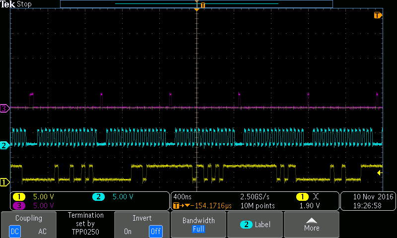
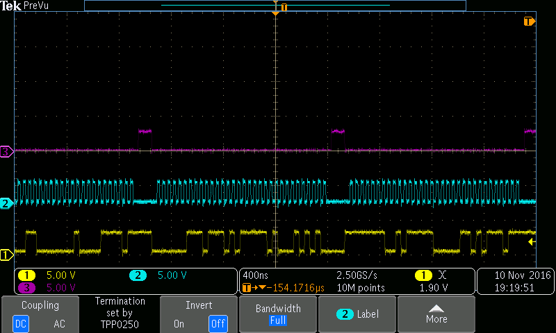
Here is a view showing the CS (magenta), CLK (blue) and MOSI (yellow):

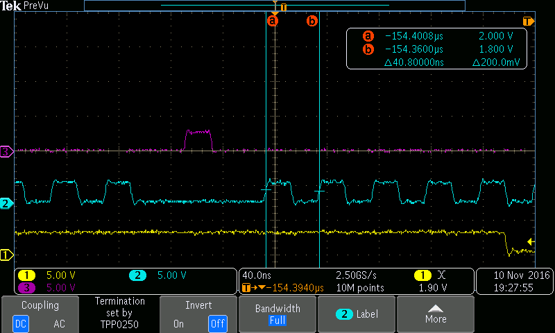
Clock cycle measurement, showing more than 40ns clock cycle time:

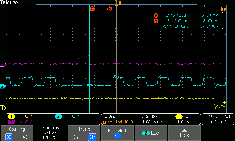
Timing from chip select assert to first clock edge (OMAP requirement seems to be 5.88ns)

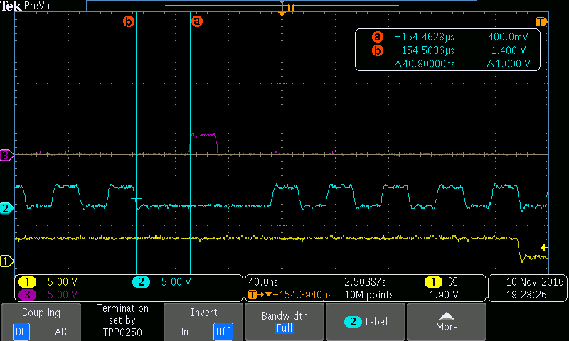
Timing measurement for last clock edge to CS de-assert (OMAP requirement seems to be 8.4ns)

I have tried modifying the master behaviour (register settings) to essentially concatenate the SPI words, i.e. one 16-bit transfer directly after the other, but the OMAP SPI peripheral almost immediately flags a TX error under these conditions.

Here is a capture, showing the 2x 16-bit transfers that almost immediately causes an issue:

1) Is there an OMAP limitation of running continuous 25MHz SPI operation, i.e. a continuous clock?

2) What is the minimum chip select de-asserted period?

3) SYSCLK2 is 228MHz in this case. Is there any other setup that is important for the SPI peripheral to achieve this operational speed?

Here is the code to initialise the SPI0 peripheral as a slave:

//configure pins
regs->spiPc0|=SPI_SPIPC0_PINSENABLE3;	//enable SOMI,SIMO,CLK
regs->spiGcr1&=~SPI_GRC1_CLKMOD_MASTER; //slave

//configure slave pin directions
regs->spiPc1=SPI_SPIPC1_SLAVEDIR;
//select data word format 0
regs->spiDat1&=~SPI_SPIDAT1_DFSEL;
//clear CSNR[n]
regs->spiDat1&=~SPI_SPIDAT1_CSNR;

//MSB first
regs->spiFmt0&=~SPI_SPIFMT_SHIFTDIR;
//no c2TDELAY and T2CDELAY in chip select timings
regs->spiFmt0|=SPI_SPIFMT_DISCSTIMERS;
//polarity: low active
regs->spiFmt0&=~SPI_SPIFMT_POLARITY;
//phase delayed
regs->spiFmt0|=SPI_SPIFMT_PHASE;
//set valid prescale value (ignored)
regs->spiFmt0|=(2<<8);
//charlen = 16 bits
regs->spiFmt0|=0x10;

//enable overflow interrupt, bit error interrupt, data length error
regs->spiLvl |= SPI_SPILVL_OVRNINTFLG|SPI_SPILVL_BITERRENA|SPI_SPILVL_DLENERRENA;
regs->spiInt0 |= SPI_SPIINT0_OVRNINTFLG|SPI_SPIINT0_BITERRENA|SPI_SPIINT0_DLENERRENA;

Thanks

  • We now have confirmed that with an OMAP running at ~85C, the issue is much, much worse, occurring once every 5mins or so.
  • Hi,

    1) Is there an OMAP limitation of running continuous 25MHz SPI operation, i.e. a continuous clock?


    No, I couldn't find such limitation, neither in TRM, nor in Datasheeto or Errata. So the SPI should be able to achieve this.

    2) What is the minimum chip select de-asserted period?


    SPI timings are listed in 6.17 Serial Peripheral Interface Ports (SPI0, SPI1), however there is no such information disclosed in the Datasheet. I will consult the design team on this.

    3) SYSCLK2 is 228MHz in this case. Is there any other setup that is important for the SPI peripheral to achieve this operational speed?

    No, as far as I understood from Chapter 7 Device Clocking & Chapter 8 Phase-Locked Loop Controller (PLLC), spi clock is sourced by SYSCLK2.

    PS:
    Could you elaborate, which SDK (Linux or RTOS) are you using?

    Also can you check if the 3-pin mode will work correctly for you? If your external device needs CS going low to syncronize or anything, you can use a dedicated gpio for this purpose.

    Best Regards,
    Yordan
  • I'm also notifying the design team about this issue.

    Best Regards,
    Yordan
  • Is the issue observed only at 25 MHz SPI clock.
    Do you also see the issue at lower clock speeds at room temperature or is this issue observed only at higher clocks at higher temperatures?
  • Hi Yordan,

    We're running SYS/BIOS 6.42.

    To clarify, the OMAP is a slave device, so CS is driven by the external device, so a GPIO is not an option.
  • Hi Rahul,

    The issue observed in clocks ranging from 24.1 up to 24.6 MHz. The issue occurs at room temperature fairly infrequently (maybe once a hour). At 75 degrees C, the issue is occuring about once every 3 minutes.
  • Hi Yordan,

    Any news on this?

    Thanks

  • Hi,

    I've sent a reminder to the design team.

    Best Regards,
    Yordan
  • Hi Pirow
    Looks like my previous post did not make it - so will try to post again
    I have been discussing this internally - and at this point I do not have any reason to believe that we have an issue with the chip but you are running pretty close to the max clock rate supported in the datasheet - I am not aware of any other customer running at this high frequency .

    Follow up questions for you
    1) Can you share with us your timing details/interface timing information - need to better understand your setup/hold time/margins etc
    2) Do you have more clarity on the nature of failure - data loss or data corruption (incorrect sampling) , and if you are getting bit errors - is your clock source good at room/high temp ? No mismatch in received/transmitted data due to some other clock/sync issues?
    3) You see failures aggravate at high temp , any data/observation at low temp?
    4) How many units tested/how many failing?
    5) Are the failures reproducible with standalone SPI traffic - or does this only happen with all your other concurrent traffic (things we discussed in the older forum post)
  • Hello Yordan,

    1) The issue is not the setup and hold of the MOSI signal, but it is the CS timing to CLK timing. Those are detailed in the scope traces above. Even if MOSI data did not line up with the clock, it should not be flagged as a data length error.

    2) The issue (as highlighted before) is that the SPI peripheral flags a data length error for MOSI and a bit TX error for SOMI. These are indicated as BITERRLVL and DLENERRLVL in the SPILVL register. Note that the SPI peripheral seem to be discarding the received SPI word in the RX register when encountering the data length error.

    3) I would need some environmental test time to cycle to -40C. I'll update once I've done that

    4) About 10 units are showing the same symtoms

    5) It seems to be correlated with full duplex operation, i.e. both SOMI and MOSI driven concurrently. RX-only (i.e. MOSI only) seems to be fine

  • Hello Yordan,

    Any news from the design team?

    I have some additional questions:

    1) Is there any other way that a BITERR or DLENERR be generated? E.g. could anything from the EDMA engine side cause such errors? If there was a TX buffer under-run for the SPI slave on the OMAP, can it cause a BITERR?

    2) Does the OMAPs clocking change with temperature? I don't expect it to, but I want to be sure that it is an analogue effect that I am seeing, rather than digital. Temperature dependence of the problem indicates that this is an analogue problem. 

    3) Can you confirm that SPI words are discarded when a DLENERR occurs? I have inferred this behaviour, but can find a reference to this in the technical manual. Disabling this discard behaviour would have simplified so many things in our implementation, because the SPI data are actually pairs.

    Thanks

  • One additional question:
    4) Is a DMA event generated for the SPI peripheral if DLENERR occurs? This would explain the missing word if it is not generated.
  • Hi,

    This is being discussed internally. I will update the thread, when we have some solution for you.

    Best Regards,
    Yordan
  • Hi Yordan,

    Another week has gone, any news on this?

  • Hi Pirow

    At what frequency do you stop seeing the issue? Will the issue re-occur if you raised the temp higher than 75c?

    On your questions i looked through the design spec

    1) No the descriptions provided in the TRM are the only reasons you will see these errors generated. EDMA state machine will not cause these errors.

    Given you see this at high temp, with simultaneous transmit and receive, how are your ruling out listed causes of BITERR? 

    A possible reason for a bit error can be noise, a too-high bit rate/capacitive load, or another master/slave trying to transmit at the same time. Are the clock plots you have same at high temp etc?

    2) No the device is specified to work at temp specifications listed in the datasheet - there are no issues like this expected due to high temp assuming you are running the device within spec 

    3) Yes the word is discarded. There was following additional description in the SPEC for DLENERR 

    • DLEN_ERR flag will be set in SPIFLG and SPIBUF (or RXBUF) register to indicate the Data Length Error and will generate an interrupt if enabled.
    • Since the received data is incomplete, it will not be copied to SPIBUF (or RXBUF).
    • RXINT flag in SPIFLG will not be set at the end of this incomplete receive and hence no interrupt on RX completion even if enabled.
    • RX DMA REQ will not be generated even if DMA Requests are enabled.
  • Pirow
    For #4 , the response is also captured as part of my response in #3.
  • Hi Mukul,

    I cannot drop the frequency below 22MHz as the application doesn't support any data rates lower than this. 

    Sorry, I should have been clearer, 75C is the maximum ambient temperature we support, the two OMAP processors on our board are then at their maximum rated temperature of 85C.

    Note that I have confirmed that we are seeing it at -40C on multiple units as well.

    If the capacitive load was too high, I would have expected "shark-fin" clocks and signals, we are not seeing any of that. Rise and fall times are within 2ns. We've set up a logic analyzer and analyzed all the clock edges when the issue occurs and the clocks are all within specification, i.e. no clocks are faster than 40ns.

  • Hi Pirow

    Do you have scope captures at the time of failure or were the plots you shared in your original post at the time of failure?

    Even if 22 MHz is the lowest frequency your application can support - can you test/confirm that you do not see issues between 22-24 MHz?

    Regards

    Mukul 

  • Pirow,

    There are 2 very different lines of debugging here.  One is EDMA transfer possibilities and one is signal integrity issues.  I recommend that you run some tests to rule out one or the other.

    EDMA:  You mention changes to the data stream that make it fail more or less often.  If you have gaps in the writes or reads form the master, does the problem ever occur?  Is this result same at all clock rates tested?  Similarly, if only having reads or only having writes, can the transactions be packed tightly without failure?  Again, is this same at all clock rates tested?

    Signal integrity: This is not clock rate dependent - this is edge rate dependent.  You mention a series resistor on the CS line.  Why is that present?  It may be causing slower transition times.  Is there a series termination on the clock line?  If so, where is it located?  Can you cause the behavior to change by adding a small capacitor (~10pf) at the clock input to the slave?  This is not a permanent solution but can point to a problem with reflections that should be fixed by adding and tuning a series source termination on the clock line.  How far apart are the SPI master and slave?  Is there any connector between?  Are there any stubs on the clock line?  Where were the scope captures taken?  Were they close to the master or the slave or at some test connector in the middle?

    Tom