This thread has been locked.

If you have a related question, please click the "Ask a related question" button in the top right corner. The newly created question will be automatically linked to this question.

TMS32C6416 Clock Edge - Customer Issue

I have one of the C64x series DSPs on a board and found a trace with a less than ideal clock edge. We are in the process of testing a modification to the trace but wanted to get TIs input on the acceptability of the signal.


In the data sheet it specifies that the clock needs to be monotonic in nature, but we were curious to know if there are slope limits to the clock edge that must be met. 


Customer has document with details of simulations and scope captures but cannot share publicly. 


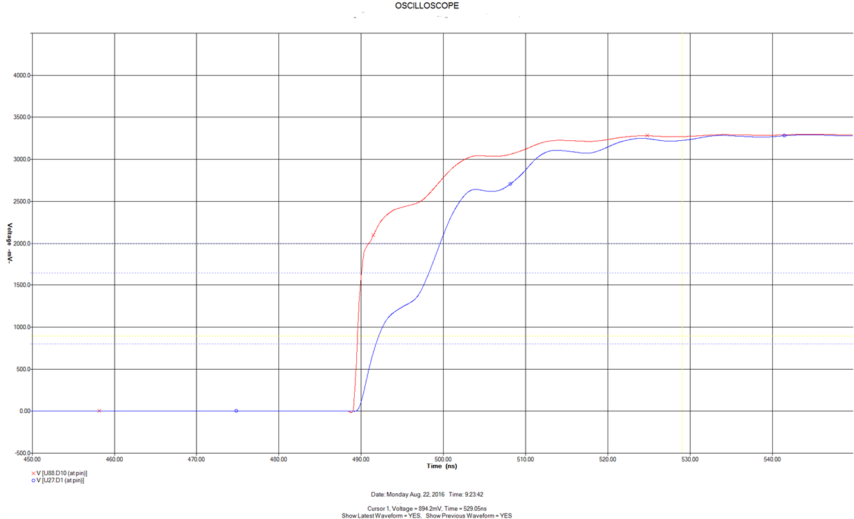
  • Please see scope capture below.

     Please see

  • David,

    These specs are in the datasheet.  The clock input transition time is limited to 5ns between VIH(min) and VIL(max).  This is on pages 76 and 80 of the datasheet.  The red line in the simulation meets that requirement and the blue line does not.

    Monotonicity is always a requirement for digital inputs.

    Tom

  • Tom,

    I am the engineer working on this, and David was nice enough to go ahead and post the question for me.

    There are a few details that should be clarified to help everybody understand the problem a little better.

    I do want to note that I did not lay this board out, this is the board that I am having to work with.

    The clock trace for a McBSP is about 14" long with several devices attached to this single trace.

    FPGA (Clock source) 2.048Mhz -> DSP -> Pin Header -> CODEC 1 -> CODEC 2

    Does this clock transition limit apply to all clocks and not just the CLKIN for the processor?  

    Also to note the red waveform is the clock source, the blue waveform is the clock at the DSP after a shunt cap was installed.

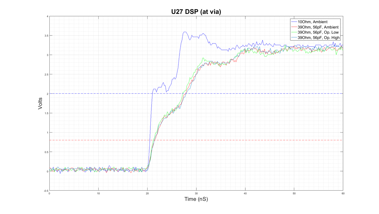
    Below is plotted data that I captured from an oscilloscope of the clock signal in question. I used a Zo probe (www.sigcon.com/.../probes.htm) tp capture the waveforms. 

    The 10ohm signal is the original signal that the designer of the schematic was focusing on. The other traces (39Ohm 56pF) are after modifications to the serial resistor and a shunt capacitor were added. 

  • The FPGA is sending a 2.048Mhz clock to the McBSP to clock data. This is not the DSP processor clock (CLKIN).
  • Michael,

    This is a very old part so support is limited.  I recommend that we assume the clock requirements for the system PLL be equally applied to the other clock inputs.  The requirements are reasonable for chips designed in these older process nodes.

    Adding load capacitance will slow the rise and fall times too much.  You are dealing with a long transmission line that ends in high impedance causing significant reflections.  I recommend use of a proper series termination resistor at the FPGA output on the order of 10-22 ohms (assuming a characteristic impedance of the line at 50 ohms).  Then I recommend a termination at the end of the transmission line.  This could be a Thevenin termination to match the characteristic impedance of the line.  Alternately, It could be an R-C to ground to minimize current consumption.  The resistor could be from 50 to 100 ohms and the capacitor could be from 22 to 100pF.  You would want to tune the values to get an appropriate rise time for the signal.

    Tom