This thread has been locked.

If you have a related question, please click the "Ask a related question" button in the top right corner. The newly created question will be automatically linked to this question.

TMS320C6746: No stable work of the DSP

Part Number: TMS320C6746

Hello!

We would like to have some help with our design.
We designed and manufactured this board and we have some problems with it. 
We manufactured 20 boards and had next problems:
1. The picture that we get from the camera that connecterd to DSP have yellow hue. Replacing camera no helped, but when at board with normal picture we replaced DSP - after replacing the picture accept yellow hue. We had 5 boards that had this issue.
2. After some time of running - there are appeared short circuit between 3.3V and GND. And after DSP replacing the short circuit disappeared. We had 3 board with this problem.
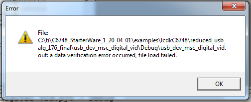
3. After some time of running the JTAG emulator couldn't connect to the board. And we get  at Code Composer next error:
After DSP replacing this issue was resolve. We had 7 boards with this problem.
4. The problem that we able to connect to the board with the emulator, but can't burn the Flash - the Code Composer give error :SPI Flash failed" And at debug/stream mode we get next error:
And if you press OK you get:
This problem we had at 4 boards. And even DSP/DDR/Flash replacing didn't helped to sort it out..
For power of the DSP we used recommended TI components and design. Here are the schematic:

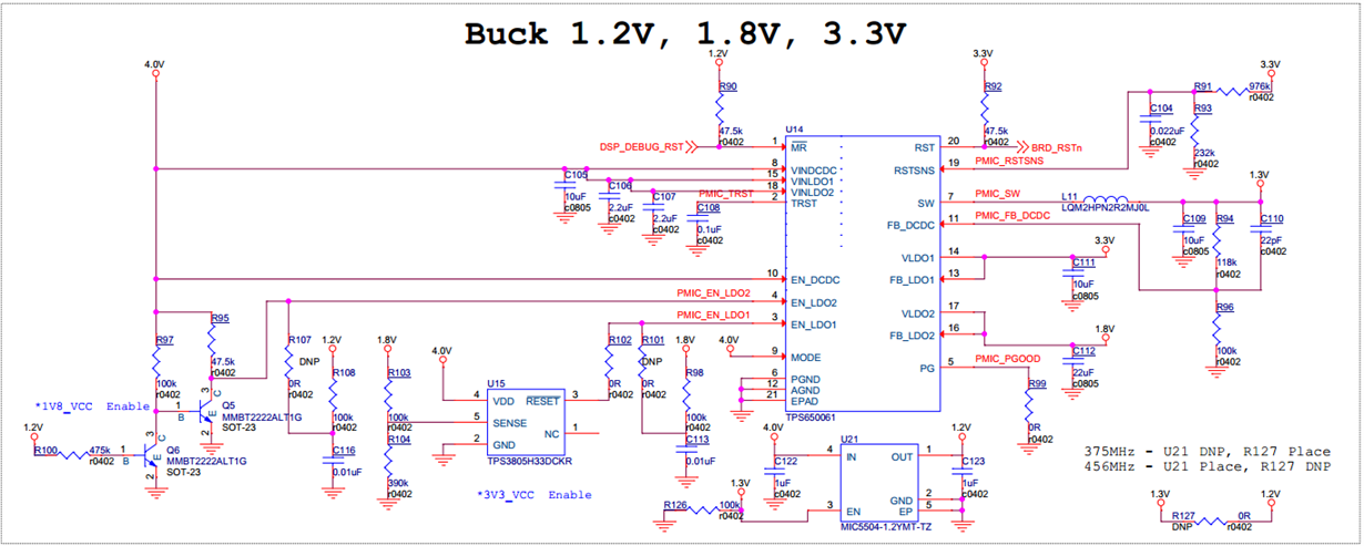
At our tests we discovered that we have exceptions at power levels, when because of noise and ripples we have at core 1.3±70mV instead of 1.3±50mV. Same problem with the 1.2V.
The possible problems that maybe make those problems are:
1. The power components placed relatively close to DSP chip - that maybe no so good for right DSP performance.
2. The area for DSP and its components is very small.
The top of layout of the DSP part is:

When we can see at top DDR K4T1G164QF-BCE7, then DSP and then power components.

The bottom of the same part of the board:

The board consists of 10 layers.
We can provide complete layout (*.brd) for review.
Can you please help us in founding possible failure points that we will take into account at the next version of our design. 
Thank you in advance

  • Hi Maxim,

    We're looking into this. Feedback will be posted here.

    Best Regards,
    Yordan
  • Hi Maxim
    Unfortunately we cannot offer schematic or layout review on public e2e.
    It would be best to try to go through the LCDK board schematic/layout and the schematic checklist to try to further isolate what may be going wrong with your board.


    If you have local TI field support, you can also check with them on if they can support you on this and the best way to move forward.
    Regards
    Mukul
  • Yes, we already contacted our TI field support.
    But always it is good to have couple of points of view.

    Anyway, can someone please answer 2 questions:

    1. What is the minimum recommended distance between DSP and main power distributor? At different TI boards we see that this distance is big and at our board it is relatively small.

    2. Is DSP proximity to the 2 board edges, as you can see at picture at the start post, can lead to DSP failures?
  • Your board does look small , but I do not think it is simple enough to say that this is the cause of potential failures.
    I am not aware of any minimum recommended distance - I will double check on this.

    For reference you can also look at the SOM module made by logic PD
    www.logicpd.com/.../

    Some relevant schematic/bom/design files can be found here (the SOM has the processor , DDR, PMIC and some other clock gen devices)

    processors.wiki.ti.com/.../OMAPL138_Univ_Kit
  • Yeah, I reviewed and compared some designs with this DSP and didn't find some critical mistakes at our design..

  • Shevchenko,

    Since all of your problems showed up on a few boards, does that mean that other boards did work correctly? Have you been able to get everything running on at least 1 board out of your 20?

    Under the assumption that some boards work okay, then we know that your schematics do not have any major problems. That would be good to know for sure. And the same for your layout, if some boards work correctly.

    There are some very thin lines of the left edge of the schematics along the DSP. That could be tough for your board shop to manufacture, and they might be having difficulties with placing the components reliably because of the small board size with the components so close to the edge.

    All of your problems that are fixed by replacing the components could easily be related to the board build and not directly to the components themselves. To verify that, I would try some of the parts you have removed on another board that has had problems. Or even remove a part on a failing board and replace it on the same board, which simply means reworking that board with the same components.

    I am certainly not a board design expert, but having your power components close to the DSP should not be a problem. If the power components were generating noise, the distance would not have a lot of effect on that noise reaching the DSP. The IR voltage drop will be reduced with shorter distances, which would be good. But the extra noise you are showing of +/- 70mV would not be related to that distance, only to the power components and filters around them. And even though that is outside the spec, it would not tend to cause this much trouble. It does need to be solved or fixed, but there must be other explanations for the problems you are having than simply power supply noise.

    Have you confirmed all the power/clock/reset sequencing is being done correctly?

    Regards,
    RandyP
  • Thank you for your reply!

    RandyP said:
    Since all of your problems showed up on a few boards, does that mean that other boards did work correctly? Have you been able to get everything running on at least 1 board out of your 20?

    Under the assumption that some boards work okay, then we know that your schematics do not have any major problems. That would be good to know for sure. And the same for your layout, if some boards work correctly.

    Yes, we have couple of boards that works good. Even I can tell more - almost all boards works well when they run at our laboratory. Majority of failure happens at customers usage.

    RandyP said:
    There are some very thin lines of the left edge of the schematics along the DSP. That could be tough for your board shop to manufacture, and they might be having difficulties with placing the components reliably because of the small board size with the components so close to the edge.

    Those lines are lines for the 2 crystals of the DSP. 

    RandyP said:
    All of your problems that are fixed by replacing the components could easily be related to the board build and not directly to the components themselves. To verify that, I would try some of the parts you have removed on another board that has had problems. Or even remove a part on a failing board and replace it on the same board, which simply means reworking that board with the same components.

    The problem with this that the main component that no work well is DSP and after replacing it is no possible to reassemble removed DSP to other board.. This is because of our components placing factory limitations.

    RandyP said:
    I am certainly not a board design expert, but having your power components close to the DSP should not be a problem. If the power components were generating noise, the distance would not have a lot of effect on that noise reaching the DSP. The IR voltage drop will be reduced with shorter distances, which would be good. But the extra noise you are showing of +/- 70mV would not be related to that distance, only to the power components and filters around them. And even though that is outside the spec, it would not tend to cause this much trouble. It does need to be solved or fixed, but there must be other explanations for the problems you are having than simply power supply noise.

    Yeah we also thought that is no need to be so critical but anyway wanted to ensure this..

    RandyP said:
    Have you confirmed all the power/clock/reset sequencing is being done correctly?

    Power/reset sequencing was checked and confirmed. And clock sequencing - I didn't saw that this DSP need to have some of it. Is it need? The clocks seems a little distorted but is this is the problem for the design?

    Thank you

  • Shevchenko,

    Shevchenko Maxim said:
    almost all boards works well when they run at our laboratory. Majority of failure happens at customers usage.

    From what you have observed with the tests in your laboratory compared with the customer usage, is there a big difference in what programs/applications are run on the DSP? Or is the environment the biggest difference, such as vibration, temperature, outside electrical noise?

    Shevchenko Maxim said:
    Those lines are lines for the 2 crystals of the DSP. 

    The chance for noise and cross-talk between long thin lines would make me nervous, especially on high-impedance lines to a crystal. I expect you have board analysis that shows it to be okay, but something to keep in mind. Problems here would tend to cause instability in the clock and might be more likely to show erratic behavior than predictable failures.

    Shevchenko Maxim said:
    The problem with this that the main component that no work well is DSP and after replacing it is no possible to reassemble removed DSP to other board.. This is because of our components placing factory limitations.

    There are ways to re-ball the DSP. I have heard of this with other customers and with our FA department. There could be a contractor in your area who can do that, but it might not be worth the trouble or expense. It is a useful way to narrow down the problem. But I can assure you that our devices are well tested before they leave our factory, so faulty DSPs are rare.

    Shevchenko Maxim said:
    Power/reset sequencing was checked and confirmed. And clock sequencing - I didn't saw that this DSP need to have some of it. Is it need? The clocks seems a little distorted but is this is the problem for the design?

    The requirements are called out in the datasheet. There is a specific order for the several power supplies, as you have already checked against. For the clock, it needs to be stable a certain time before RESET and TRST can be released. This is not as complex as some of our devices, so my terminology may be a bit strong to call it 'sequencing', but the clocks do have to be stable before releasing RESET.

    Is it true that the boards work under laboratory testing first, then they go to the customer for testing and some fail there? And then do they continue to fail your original tests when you bring them back to your laboratory? That is how I read you comments above. Do you have any observations to share about the condition of the boards when returned? Or about how they are used at the customer's site?

    Regards,
    RandyP

  • RandyP said:
    From what you have observed with the tests in your laboratory compared with the customer usage, is there a big difference in what programs/applications are run on the DSP? Or is the environment the biggest difference, such as vibration, temperature, outside electrical noise?

    At the lab we run same programs as at customer place. I don't know about big differences at environment. The only difference is that customer use one more board in order to connect to DSP. I will explain this:

    Because there are no place for JTAG at the main board, we made additional two boards - Debug Adapter where the DSP JTAG is placed and DSP connector - the board that connected to main board when the product is at his package. So the DSP can be connected in 2 ways:

    1. Main board connected with flex cable to Debug Adapter Board on which JTAG connector placed.

    2. Main board connected with flex cable to Debug Connector Board, that connected with small HDMI cable to Debug Adapter board on which JTAG connector placed.

    At the lab we mainly work with possibility number 1, and customer with possibility number 2. However we made couple of tests with possibility number 2 at the lab and it worked fine.. But it was no with high density of usages as customer did.

    We also found some error with those 2 additional boards when we found that the distance between DSP and JTAG header need to be no more than 6 inch. At possibility 1 the distance between DSP and JTAG is around 6 inch, but at number 2 is more than 2 inch. At next version of the Debug Adapter and Debug Connector we will add buffers as recommended by TI. 

    Is this mistake can lead to so much DSP failures?

    RandyP said:
    There are ways to re-ball the DSP. I have heard of this with other customers and with our FA department. There could be a contractor in your area who can do that, but it might not be worth the trouble or expense. It is a useful way to narrow down the problem. But I can assure you that our devices are well tested before they leave our factory, so faulty DSPs are rare.

    Do you heard about same problems with this DSP elsewhere? I found at Internet some threads with one of my problems - but there no solution except link for hardware check on TI Wiki.

    RandyP said:
    The requirements are called out in the datasheet. There is a specific order for the several power supplies, as you have already checked against. For the clock, it needs to be stable a certain time before RESET and TRST can be released. This is not as complex as some of our devices, so my terminology may be a bit strong to call it 'sequencing', but the clocks do have to be stable before releasing RESET.

    I tested this now and it works as needed.

    RandyP said:
    Is it true that the boards work under laboratory testing first, then they go to the customer for testing and some fail there? And then do they continue to fail your original tests when you bring them back to your laboratory? That is how I read you comments above. Do you have any observations to share about the condition of the boards when returned? Or about how they are used at the customer's site?

    The boards that return to our laboratory many time seems to be very weared out, at some boards there are no camera because the customer didn't insert in good way the board to it packaging. At lab all was very soft and customer seems to use very hard the boards.

  • Hello!

    Is someone have new thoughts about our issue?

    Which tests can I do to my board except standard board tests to determine what is the problem?

    Thank you

  • Shevchenko,

    One way to rule out clock noise or power supply noise as the cause would be to disable the on-board clock and / or the power supplies and to wire in bench supplies for these supply rails.  if this resolves a board that has the problems, this proves that the power and / or clock implementation is the cause.  Please let us know the results of this test.

    Tom

  • We removed power components and insert external power to DSP voltages. At the board we still see the problematic ripple when on output of power supplies it is ok.

  • Shevchenko,

    This appear to indicate that your decoupling implementation is not adequate.  Are you using small capacitors with low ESL ?  Do you have the sufficient quantity of the recommended values?  Are the caps with short and wide traces resulting in low PCB inductance?  You should be able to modify your board to get the power supply noise down to the required level.  Note that the wires from the bench supplies need to be as short as possible to minimize inductance and a large cap may need to be added at the connection point for these wires.

    You did not indicate whether use of the bench supplies affected the system issue reported (picture with yellow hue).  Was there any effect?

    Tom

  • We used quantities, recommended values and kind of capacitors as we saw at one of evaluation boards, we also checked it with decoupling recommendations of TI. The traces are short as possible.

    We didn't try to make bench supplies to board with picture with yellow hue

    Thank you

  • Shevchenko,

    The point of this exercise is to determine the contributing factors to the yellow hue problem.  Please rework one of these boards to operate with the bench supplies to see if this resolves the reported problem.

    Tom

  • Hello to all!

    As the issue back to e2e forum it is better to continue discussion here.

    Since the last update we manufactured 5 new boards at different components assembly place.
    We also manufactured new Debug Adapter board with recommended buffers configuration.

    1. All 5 boards had good picture from camera, without yellow hue.
    2. All 5 boards succeed to connect to DSP via JTAG at the beginning and worked fine.
    3. After some time one of the boards stopped work. And after checking was found that DSP hold TCK pin at "1" all the time. And short time after it another board failed to connect via JTAG and was found that TMS pin hold at "1" by DSP. Seems that protective diodes of IO's was damaged..
    We found that the their exist possibility that signals came to DSP IO's before the DSP power supply. So we changed the DSP debugging procedure in order that it will ensure that signals will come after the power supplies. But in this way 3 other boards after 10-20 cycles of connection at the end got damaged at same way..

    So we see that the main problem is at connectivity between DSP and debugger.

    Which tests can help us to resolve this issue?

    Thank you.
  • Shevchenko,

    I would look at your "Debug Adapter board with recommended buffers configuration". If that board was driving the JTAG signals on the DSP prior to power being applied to the DSP, then that is the likely point of fault. It is possible that the boards were damaged before the change to your debugging procedure.

    But that is not really possible to tell. We do not know about your board+adapter design or changes or debug procedures in order to comment on those. Or which JTAG pod you are using.

    Regards,
    RandyP
  • Shevchenko,

    Randy has indicated the probable cause of device damage.  You can change the circuitry on the debug board to prevent it from driving the pins on the DSP before it is powered.  Emulators and debuggers routinely monitor the TVD (target voltage detect) pin and do not drive ant pins until the target is powered.

    Tom

  • Hello!

    Yes, we thought about this possibility. So lately we changed that Debug Adapter Board buffers, JTAG and other components that driving signals to DSP - get their 3.3V from the Main Board and no from external source. For now it looks that it helped. 4 boards looked to work fine and no get damaged. But need to verify this with more. We send damaged boards to DSP rework, will test it and find out is this was the issue.

    Thank you