This thread has been locked.

If you have a related question, please click the "Ask a related question" button in the top right corner. The newly created question will be automatically linked to this question.

TMS320C6748: uPP receiver IO impedance

Part Number: TMS320C6748

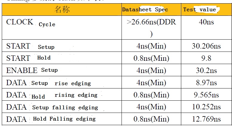
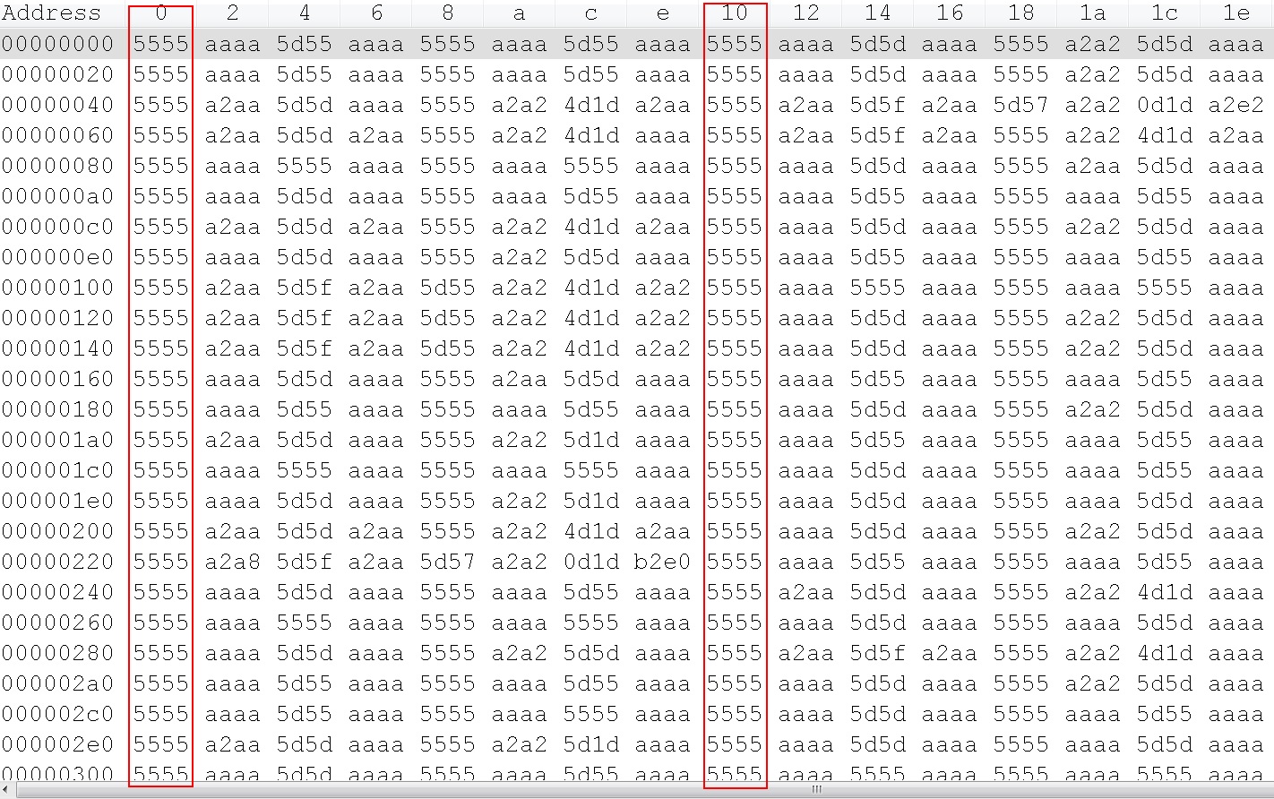
Customer used uPP DDR receive mode, there are some stability issue on few boards after MP, change the data line serial resistor from 20ohm to 50ohm, the error rate decreased, so customer ask the real IO impedance?

  • Hi Tony,

    I couldn't find this in the public documents. I've notified the design team. They will post directly here.

    Best Regards,
    Yordan
  • Hi Tony,

    I have a couple of follow up questions to help me better understand the situation:
    1. What do you connect on the UPP bus? If you share what is the chip, then I may be able to find some useful info in its datasheet.
    2. How do you connect the series resistor? Close to the host? Or close to the device?
    3. What is the impedance of the PCB lines for uPP in your custom board?

    Best Regards,
    Yordan
  • Yordan Kovachev said:
    1. What do you connect on the UPP bus? If you share what is the chip, then I may be able to find some useful info in its datasheet.

    It is FPGA, I don't have the part number, if you think it is important, I will try to get the part number.

    Yordan Kovachev said:
    2. How do you connect the series resistor? Close to the host? Or close to the device?

    on the source side, so it is on FPGA side as DSP uPP in receive mode.

    Yordan Kovachev said:
    3. What is the impedance of the PCB lines for uPP in your custom board?

    Customer told me it is 50ohm, not sure the PCB manufacture error.

    paste some test data for you reference.

    #1. with 20ohm resistor, sent from FPGA 0x5555 and 0xAAAA alternately,  every 8 data(16bit uPP) are right. there are some bit error in other slot data.

    #2. change resistor from 20ohm to 50ohm, odd channel data are right(red frame), even channel has some bit error(blue frame). (the data in below snapshot is decimal, send from FPGA: 800, 700, 600, 500, 400, 300, 200 100 in sequence)

    So I think the problem related to impedance. and I am not sure whether it relate to cross talk or there is a period interference impacted the uPP data signal, maybe increased serial resistor value consumed the interference energy, and result in the error pattern change.

  • Hi,

    It is FPGA, I don't have the part number, if you think it is important, I will try to get the part number.
    Customer told me it is 50ohm, not sure the PCB manufacture error.


    I think the load from TMS320C6748 pads should not be that different to cause impedance mismatch, considering that the interface works at approx. 38 MHz and I imagine traces are not that long.

    on the source side, so it is on FPGA side as DSP uPP in receive mode.


    This should be correct.

    As for the cross-talk I can't say. Can you try playing with the FPGA slew rate (increase or decrease if possible)?
    Also this could be a sw issue. Is it possible to try and run their application at lower speeds? Review the timings; make sure that the fpga interface matches the timings from the dsp datasheet.

    Best Regards,
    Yordan
  • Yordan,

    Thanks. More background: uPP receive works in DDR mode with 25MHz uPP_CLK.

    #1. This product shipped ~15K units, so far found ~5pcs board return with this issue, these board worked fine for >1year in field before report such issue. 

    #2. debug these returned  board:

    #2.1 We did lower uPP_CLK from 25MHz to 12.5MHz, error disappear.

    #2.2 Change uPP timing to align uPP_CLK and uPP_data, error disappear. from spec, uPP_CLK should a liitle ahead of other signals. so the wrong timing works, but the right timing cause error. the original timing send from FPGA as below snapshot, the setup and hold time meet uPP timing requirement. (you can ignore the wave SI quality as poor grounding of probe)

    #2.3 All boards run the same software.

    #2.4. Customer said he has adjusted FPGA load capability with different value, error remain. (they did not capture if error rate/patter change along FPGA IO load change).

    #2.5 Replace the DSP with a new one, error disappear, but did not solder back the failure DSP to another board as repair line dropped it.

    #2.6. Change uPP_data line serials experiments and result as previous post.

    Thanks for analysis.

  • Hi,

    Have you tested "#2.1 We did lower uPP_CLK from 25MHz to 12.5MHz, error disappear." & "2.2Change uPP timing to align uPP_CLK and uPP_data, error disappear" extensively? Can you consider these as possible workarounds? It seems that this is some sort of timings issue, but i cannot be sure if this comes from the DSP or the FPGA... I know this may be very time consuming, but is it possible to experiment with the same timings but connect two DSPs through uPP, if you don't get the error then you should consider adjusting the timings from FPGA side.

    Best Regards,
    Yordan
  • Yordan,

    The stored test data file upto several Mbyte, so we think it is extensively tested.

    Yordan Kovachev said:
    Can you consider these as possible workarounds?

    No, low uPP_CLK can't meet requirement. The aligned uPP_CLK and uPP_Data doesn't meet uPP spec timing, otherwise TI guarantee the aligned timing meet  spec and modify datasheet.

    And that is why customer request TI help to figure out the root cause.

    Yordan Kovachev said:
    but is it possible to experiment with the same timings but connect two DSPs through uPP, if you don't get the error then you should consider adjusting the timings from FPGA side.

    it is not doable, firstly it is not a common issue, just several pcs out of 15Kunit. secondly, it is on customer board.

  • Hi Tony,

    otherwise TI guarantee the aligned timing meet spec and modify datasheet.

    I don't think this is a possibility. Ok, on the failed products can you replace the FPGA then to see if the problem is solved again?

    Have you explored the possibility of poor mounting of the DSP (or FPGA) on the board (xray)?
    As I said this could be a timing issue (maybe setup or hold time is not within specs)... How long are the upp traces? I assume the FPGA and the DSP are on the same board.

    You said the failed boards have worked in the field for over a year. Did something abnormal happened when they were functioning...

    I am running out of ideas. I will try to find someone in the design team to elaborate.

    Best Regards,
    Yordan
  • The wave is post in previous.

    below is the timing data, it is within spec with large margin.

  • Hi Tony,

    I've consulted the design team. I am waiting for some feedback.

    Best Regards,
    Yordan
  • Hi Tony,

    You seem to have a timing issue on particular bits. This may be a layout problem due to trace length or cross talk or it may be an issue with the timing constraints within the FPGA. You captured D15 on the your plots but bit doesn't appear to be one that is failing. On the failing boards, do you find that the same bits are causing problems? Can you captured the wave form on one of the bits that is failing consistently as close to the SOC as possible? Can you capture more then one of the data bits to see if there is any significant skew between the the edges? Another issue with FPGA implementations is the timing constraints within the FPGA design. Can you provide the constraint that defines the allowable skew at the output of the FPGA?  

    Regards, Bill

  • Hi Tony
    On digging further in the design specs for the dual LVCMOS IO buffers used in the UPP , the values I found were

    for 1.8V operation -
    Nominal Impedance Value is ~33 ohm
    or 3.3 V operation -
    Nominal Impedance Value is ~35 ohm

    Nominal is room temp , nominal process

    The worst case across operating conditions is
    for 1.8V operation - ~50 ohm
    For 3.3 V operation - ~ 57 ohm.