This thread has been locked.

If you have a related question, please click the "Ask a related question" button in the top right corner. The newly created question will be automatically linked to this question.

A question about using C6748's SPI1 as SPI Slave

Other Parts Discussed in Thread: TMS320C6748, OMAPL138

Dear All,

I have a question about using C6748's SPI1 as SPI Slave.

I can successfully  receive data from SPI Master. However, I failed to correctly send data to it.

What I expect to send on MISO is:

63_21_43_65 => 0110_0011_0010_0001_0100_0011_0110_0101

                6    3    2    1    4    3    6    5

But it turns out the actual waveform on MISO is:

0C_64_28_6C => 0000_1100_0110_0100_0010_1000_0110_1100
                0    C    6    4    2    8    6    C

The waveform seem to have 3-bit "delay" (The 3 zero highlighted in red) compared to what I expected.

You can see the waveform here:


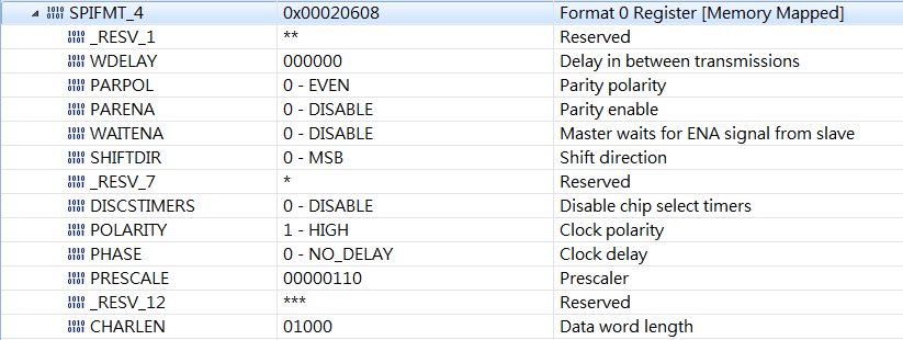
And you can see the settings of the SPIFMT0 register here:


Originally I assume that if my FW sends data too late, then the delay on MISO will be "byte-aligned", i.e.,

delay will be 1-byte, 2-byte, etc. However, it seems that my assumption is not correct, right?

Any comment will be highly welcome!

Regards,

Oliver

  • Dear All,

    I suspect this symptom occurs because I can't control SPI Transmitter to send data in a byte-aligned way.

    I modified my FW to improve its execution performance, then I was surprised to see that the desired TX data

    appears on MISO pin few clocks EARLIER then I expected.

    In the following waveform you can see the D4/D5 (please check the SDO part of the bottom SPI protocol analyzer)

    are 0x03/0x18. However, they should be 0x00/0x63. In other words, the TX data appears on MISO is 3 clocks earlier

    then I expected.

    Could anyone check this issue and comment?

    Regards,

    Oliver

  • Hello Oliver,

    Are you using TI EVM or custom board ?
    Are you using TI provided example code or your own code ?
    What change you have done in FW to improve the performance ?
    Are you able to reproduce this issue ?

    Regards,
    Senthil
  • Dear Senthil,

    First thanks for your reply.

    I'm using a custom board and use my own code.

    My changes that improve performance is simply replacing the computation of some register addresses

    at run-time with the result address in order to save the computation time.

    Yes, I can reproduce this issue if I want.

    If you are interested, below is that part of code:

    #define SPI1_SPIFLG  (0x01F0E010)
    #define SPI1_SPIBUF  (0x01F0E040)
    #define SPI1_SPIDAT1 (0x01F0E03C)

    {

    // Wait for Command code

    //

    while (!( HWREG(SPI1_SPIFLG) & SPI_SPIFLG_RXINTFLG ));

    // Read Command code

    //

    rxdat [0] = (unsigned char) (HWREG(SPI1_SPIBUF) & SPI_SPIBUF_RXDATA);

    }

    // Receive Address: 3 bytes

    //

    {

    // Wait for Address byte 2 to arrive

    //

    while (!( HWREG(SPI1_SPIFLG) & SPI_SPIFLG_RXINTFLG ));

    // Read Address byte 2

    //

    rxdat [1] = (unsigned char) (HWREG(SPI1_SPIBUF) & SPI_SPIBUF_RXDATA);

    // Wait for Address byte 1 to arrive

    //

    while (!( HWREG(SPI1_SPIFLG) & SPI_SPIFLG_RXINTFLG ));

    // Read Address byte 1

    //

    rxdat [2] = (unsigned char) (HWREG(SPI1_SPIBUF) & SPI_SPIBUF_RXDATA);

    // Wait for Address byte 0 to arrive

    //

    while (!( HWREG(SPI1_SPIFLG) & SPI_SPIFLG_RXINTFLG ));

    // Read Address byte 0

    //

    rxdat [3] = (unsigned char) (HWREG(SPI1_SPIBUF) & SPI_SPIBUF_RXDATA);

    }

    // Transmit data: 4 bytes

    {

    // Write Data byte 0

    //

    HWREG(SPI1_SPIDAT1) = (unsigned int)txdat[0];

    // Wait for Transmitter empty

    //

    while (!( HWREG(SPI1_SPIFLG) & SPI_SPIFLG_TXINTFLG ));

    // Write Data byte 1

    //

    HWREG(SPI1_SPIDAT1) = (unsigned int)txdat[1];

    // Wait for Transmitter empty

    //

    while (!( HWREG(SPI1_SPIFLG) & SPI_SPIFLG_TXINTFLG ));

    // Write Data byte 2

    //

    HWREG(SPI1_SPIDAT1) = (unsigned int)txdat[2];

    // Wait for Transmitter empty

    //

    while (!( HWREG(SPI1_SPIFLG) & SPI_SPIFLG_TXINTFLG ));

    // Write Data byte 3

    //

    HWREG(SPI1_SPIDAT1) = (unsigned int)txdat[3];

    // Wait for Transmitter empty

    //

    while (!( HWREG(SPI1_SPIFLG) & SPI_SPIFLG_TXINTFLG ));

    }

    Any other comment?

    Regards,

    Oliver

  • Hello Oliver,

    In hardware point of view, Did you try using termination resistor and check the transactions ?

    What is the length difference between SPI clock and SOMI ?

    Regards,

    Senthil

  • Dear Senthil,
    No, there is no termination resistor because the SPI clock is only 17MHz.
    By "check the transactions", do you mean to check the waveform using an oscilloscope?

    And, by "length difference between SPI clock and SOMI", I guess you mean the "trace length"
    difference of these two signals? I'm not sure what this difference is. However, as the
    execution time of my FW code will determine whether the TX data will appear on MISO earlier
    or later then I expected, I guess this difference may not the root cause of this symptom.

    So maybe I should state my question in another way: Under normally condition, SPI
    Transmitter will send TX data to MISO pin is a byte-aligned (every 8-SPI-clock,
    when SPIFMT0's CHARLEN is set to 8-bit) way, no matter how late or how early FW code
    writes data to SPIDAT1's TXDATA, right?

    Regards,

    Oliver
  • Hello Oliver,

    No, there is no termination resistor because the SPI clock is only 17MHz.
    By "check the transactions", do you mean to check the waveform using an oscilloscope?

    Yes, i meant to check the waveform using scope/LA.

    And, by "length difference between SPI clock and SOMI", I guess you mean the "trace length"
    difference of these two signals? I'm not sure what this difference is. However, as the 
    execution time of my FW code will determine whether the TX data will appear on MISO earlier
    or later then I expected, I guess this difference may not the root cause of this symptom. 

    So maybe I should state my question in another way: Under normally condition, SPI 
    Transmitter will send TX data to MISO pin is a byte-aligned (every 8-SPI-clock, 
    when SPIFMT0's CHARLEN is set to 8-bit) way, no matter how late or how early FW code 
    writes data to SPIDAT1's TXDATA, right?

    Inspite of byte-aligned, you are seeing 3 bit delay on MISO pin. So i suspect the trace length difference between CLK and MISO could create this issue. Please ensure the trace length difference is minimal.

    Regards.

    Senthil

  • Dear Senthil,
    Thanks for your comment.

    I always connect an LA to monitor the SPI Bus activities. However, I can't find any suspicious noise that could result in this symptom.

    The trace length difference between SPI Clock and MISO is less than 1cm. For a synchronous circuit running at 17MHz (58.8ns period), I assume such difference won't result in timing variation as long as 3 clocks (176ns).

    To get a better idea about whether this trace length is the root cause or not, I modified my FW code such that SPI Transmitter will send data from the very beginning of an SPI transaction. In this way the data appears on MISO will be exactly what I expect. I think such result excludes the trace length difference from being the root cause of this symptom. 

    I'm wondering whether there is any register controlling the "byte-aligning" nature of SPI Transmitter? And, do you have any other comment?

    Regards,

    Oliver

  • Hi Oliver,

    1)

    Oliver says said:

    I modified my FW to improve its execution performance, then I was surprised to see that the desired TX data

    appears on MISO pin few clocks EARLIER then I expected.

    What did you change for getting the data earlier ?

    Any registers ?

    Please check the "DESYNCFLG" bit from SPIFLG register at master side.

    2)

    Oliver says said:

    To get a better idea about whether this trace length is the root cause or not, I modified my FW code such that SPI Transmitter will send data from the very beginning of an SPI transaction. In this way the data appears on MISO will be exactly what I expect. I think such result excludes the trace length difference from being the root cause of this symptom.

    What FW modification you made ?

    Could you please attach the code with comments what you modified for above both conditions.

    Did you modify any register for that both conditions (1 & 2)

  • Dear Titus,

    Below check my answers to your questions:

    1)

    Q.1.1 What did you change for getting the data earlier ?

    What I changed is only the way of writing the code controlling registers. Here is an example of the original code:

    HWREG(baseAdd + SPI_SPIDAT1) = (HWREG(baseAdd + SPI_SPIDAT1) & ~ SPI_SPIDAT1_TXDATA) | txdat[0];

    I changed it to:

    HWREG(SPI1_SPIDAT1) = (unsigned int)txdat[0];

    This will shorten the executing time of writing data to the SPIDAT1 register.

    Q.1.2 Any registers ?

    If you mean: "Do you change any register for getting the data earlier", then the answer is No.

    All the registers I access using the original way and the new way are the same. The difference is the "style" of writing the FW code I explained in Q.1.1

    Q.1.3 Please check the "DESYNCFLG" bit from SPIFLG register at master side.

    DESYNCFLG is 0, No error.

    According to P.1377 of TMS320C6748 DSP Technical Reference Manual, it says: "Desynchronization monitor is active in master mode only." I assume this bit is irrelevant in my case because my SPI1 works as SPI Slave.

    2)

    Q.2.1 What FW modification you made ?

    Before I explain what FW modification I made, let me explain what I did in my FW for a SPI transaction:

    Step 1. Assert some signal (some GPIO signal) to Host to notify it that I'm ready to receive an SPI command

    Step 2. Receive a sequence of 4 bytes from SPI Master

    Step 3. Transmit a sequence of 4 bytes to SPI Master

    The modification I did was simply switching the order of Step 2 and 3.


    Q.2.2 Could you please attach the code with comments what you modified for above both conditions.

    No problem.

    The lines in red/green/blue background are for Step. 1/2/3 mentioned in my answer to Q.2.1

    ASSERT_INT_TO_HOST;

    // Receive Command code: 1 bytes
    //
    {
    // Wait for Command code
    //
    while (!( HWREG(SPI1_SPIFLG) & SPI_SPIFLG_RXINTFLG ));

    // Read Command code
    //
    rxdat [0] = (unsigned char) (HWREG(SPI1_SPIBUF) & SPI_SPIBUF_RXDATA);
    }

    // Receive Address: 3 bytes
    //
    {
    // Wait for Address byte 2 to arrive
    //
    while (!( HWREG(SPI1_SPIFLG) & SPI_SPIFLG_RXINTFLG ));

    // Read Address byte 2
    //
    rxdat [1] = (unsigned char) (HWREG(SPI1_SPIBUF) & SPI_SPIBUF_RXDATA);

    // Wait for Address byte 1 to arrive
    //
    while (!( HWREG(SPI1_SPIFLG) & SPI_SPIFLG_RXINTFLG ));

    // Read Address byte 1
    //
    rxdat [2] = (unsigned char) (HWREG(SPI1_SPIBUF) & SPI_SPIBUF_RXDATA);

    // Wait for Address byte 0 to arrive
    //
    while (!( HWREG(SPI1_SPIFLG) & SPI_SPIFLG_RXINTFLG ));

    // Read Address byte 0
    //
    rxdat [3] = (unsigned char) (HWREG(SPI1_SPIBUF) & SPI_SPIBUF_RXDATA);
    }

    // Transmit data: 4 bytes
    {
    // Write Data byte 0
    //
    HWREG(SPI1_SPIDAT1) = (unsigned int)txdat[0];

    // Wait for Transmitter empty
    //
    while (!( HWREG(SPI1_SPIFLG) & SPI_SPIFLG_TXINTFLG ));

    // Write Data byte 1
    //
    HWREG(SPI1_SPIDAT1) = (unsigned int)txdat[1];

    // Wait for Transmitter empty
    //
    while (!( HWREG(SPI1_SPIFLG) & SPI_SPIFLG_TXINTFLG ));

    // Write Data byte 2
    //
    HWREG(SPI1_SPIDAT1) = (unsigned int)txdat[2];

    // Wait for Transmitter empty
    //
    while (!( HWREG(SPI1_SPIFLG) & SPI_SPIFLG_TXINTFLG ));

    // Write Data byte 3
    //
    HWREG(SPI1_SPIDAT1) = (unsigned int)txdat[3];

    // Wait for Transmitter empty
    //
    while (!( HWREG(SPI1_SPIFLG) & SPI_SPIFLG_TXINTFLG ));
    }


    Q.2.3 Did you modify any register for that both conditions (1 & 2)

    No. Only switching the order of Step. 2 & 3.

    Any comment?

    Regards,

    Oliver

  • Dear Titus,
    As I haven't received your response, I assume this issue is quite unusual. I'm wondering if it is caused by some bug of C6748's SPI Controller when it is configured as SPI Slave?
    If not, could you provide the on-board verification condition of C6748's SPI Controller when it is configured as SPI Slave, so I can try to duplicate the same verification on our board?
    Or, could you provide any verified simple sample code that enables C6748 to communicate with SPI Master, so I can port it to our board to see if I can get the same result or not?

    How do you think?

    Regards,

    Oliver
  • Hi Oliver,

    I modified my FW code such that SPI Transmitter will send data from the very beginning of an SPI transaction. In this way the data appears on MISO will be exactly what I expect. I

    In this statement, you said, I can see the data what I expect right,
    Able to get expected behavior when you transmit the data very beginning of an SPI transaction ?

    Actually we don't have a example code for SPI slave.
    I have seen some customers that they have used SPI slave in C6748/OMAPL138 without any problem.
  • Dear Titus,
    If I have SPI Transmitter send data, e.g., 0x63, at the beginning (the first byte) of an SPI transaction (there should be totally 9 bytes), then the data appears on MISO will be exactly 0x63 without and delay. That is, 0x63 will be on the 1st byte.
    Unfortunately, I need to send the data on the 5th byte of this transaction instead of the 1st one, and I still fail to align that data 0x63 to the 5th byte. The 8 bits (0110_0011) of 0x63 always appear in two consecutive bytes.

    Since you've seen your customers using C6748's SPI slave without any problem, then that API controller should be OK. If you don't have any SPI Slave sample code on hand, how about I send you a pack of highly simplified code that can duplicate this symptom?
    If you have an C6748 board with connection to SPI1 or SPI0 signals and an SPI Master with 17MHz clock, then you should be able to test this code.

    How do you think?

    Regards,

    Oliver
  • Hi Oliver,
    I will try to reproduce this behavior on OMAPL138 LCDK board and let me update.
  • Dear Titus,

    OK, it's a good idea. Please inform me if you get the result.

    Thanks in advance!

    Regards,

    Oliver

  • Hi Oliver,

    What is your SPI Master Device ?
    If your OMAPL138 is SPI slave then who is your SPI master ?
    Are you communicating on Two different boards ?

    Please make sure the correct initialization is done for both SPI Master and Slave.
    For that please refer Chapter 28.2.19 of C6748 Technical reference manual.

  • Dear Arvind,

    Finally this issue was solved yesterday. The key is: We got to start to transmit in the very beginning of each SPI transaction instead of in the middle of it. And, it's also necessary to stuff 2 pcs (stuff the 2nd one right after the 1st one is in TX shift register) of data before waiting to receive the first data.

    In this way we can align every transmitted data to a byte.

    Thanks for all your help!

    Regards,

    Oliver

  • Hello Oliver,

    Glad to know that your issue is resolved. Thanks for the update.

    Regards,
    Senthil