This thread has been locked.

If you have a related question, please click the "Ask a related question" button in the top right corner. The newly created question will be automatically linked to this question.

C6745 GPIO problem

Hello.

I have C6745 DSK and cslr library.

 My GPIO example working only when:

/** @brief Base address of GPIO memory mapped registers */
#define CSL_GPIO_0_REGS (0x01E26000u)

but in  [SPRS377F – SEPTEMBER 2008–REVISED JUNE 2014] document we have the next:


Where is a mistake?

2) I am using Bank_1 -> Pin_5

When i write:

 /* Configure GPIO1_5 (GPIO1_5_PIN) as an output */
 gpioRegs->BANK[1].DIR &= ~(CSL_GPIO_DIR_DIR_IN << CSL_GPIO_DIR_DIR5_SHIFT);  - it is not work

but when i write the next:

 /* Configure GPIO1_5 (GPIO1_5_PIN) as an output */
 gpioRegs->BANK[0].DIR &= ~(CSL_GPIO_DIR_DIR_IN << CSL_GPIO_DIR_DIR21_SHIFT); - it is work fine

Is it correct ?

What values takes  X   in    BANK[X].DIR ?

Where it can be read ?

  • Hi Alex,

    SPRS377F datasheet is common for both C6747 and C6745.
    In C6747 USB1 is present which uses address 0x01E25000 but this peripheral is not present in C6745,So these address are kept unused in C6745.
    You can cross verify GPIO address in datasheet's chapter 6.8 (General-Purpose Input/Output) in datasheet itself.

    What values takes X in BANK[X].DIR ?

    Here X corresponds to the bank which you are using, For example
    X=0 for bank 0
    X=1 for bank 1 etc

    Where it can be read ?

    By reading the pin name itself you will get to know to which bank that pin belongs to.
    for example,
    If pin name is GP0[12] - It belongs to Bank 0. Means here 'X' value will be 0.
    If pin name is GP2[1] - It belongs to bank 2. Means here 'X' value will be 2.
  • Ok , thank for your help.

    I continued to experiment with Gpio interrupt, but my source code is not work fine  (I did not get into the interrupt handler).

    LED connected to GP1[5], SW connected to GP1[4].

    Where is my mistake ? 

    #include <stdio.h>
    #include <c6x.h>
    #include <cslr_gpio.h>
    #include <cslr_syscfg_C6745.h>
    #include <soc_C6745.h>
    #include <cslr_psc_C6745.h>
    #include <cslr_dspintc.h>
    
    /*============================================================================*/
    /*                             GLOBAL VARIABLES                               */
    /*============================================================================*/
    
    /* sys config registers overlay                                               */
    CSL_SyscfgRegsOvly   sysRegs  = (CSL_SyscfgRegsOvly)(CSL_SYSCFG_0_REGS);
    /* Psc register overlay                                                       */
    CSL_PscRegsOvly      psc1Regs = (CSL_PscRegsOvly)(CSL_PSC_1_REGS);
    /* Gpio register overlay                                                      */
    CSL_GpioRegsOvly     gpioRegs = (CSL_GpioRegsOvly)(CSL_GPIO_0_REGS);
    /* Interrupt Controller Register Overlay                                      */
    CSL_DspintcRegsOvly intcRegs = (CSL_DspintcRegsOvly)CSL_INTC_0_REGS;
    
    /*============================================================================*/
    /*                        EXTERNAL FUNCTION PROTOTYPES                        */
    /*============================================================================*/
    
    extern void intcVectorTable(void);


    volatile Int32 status = 0;
    
    #define GPIO0_EVENT    65
    #define MAX_BLINK       4


    void gpioExample(void)
    {
        volatile Uint32 temp = 0;
        volatile Uint32 pscTimeoutCount = 10240u;
    
        /* Key to be written to enable the pin mux registers to be written        */
        sysRegs->KICK0R = 0x83e70b13;
        sysRegs->KICK1R = 0x95A4F1E0;
    
        /* mux between EMA_A[4] and GPIO1_4 : enable GPIO1_4 (User Switch - "SW3-1")  */
        sysRegs->PINMUX16 = ( (CSL_SYSCFG_PINMUX16_PINMUX16_11_8_GPIO1_4) << \
                            (CSL_SYSCFG_PINMUX16_PINMUX16_11_8_SHIFT) );
    
        /* mux between EMA_A[5] and GPIO1_5 : enable GPIO1_5 (User Led - "DS1")    */
        sysRegs->PINMUX16 = ( (CSL_SYSCFG_PINMUX16_PINMUX16_15_12_GPIO1_5) << \
                            (CSL_SYSCFG_PINMUX16_PINMUX16_15_12_SHIFT)  );
    
      /* Bring the GPIO module out of sleep state                                 */
      /* Configure the GPIO Module to Enable state */
      psc1Regs->MDCTL[CSL_PSC_GPIO] =
                                  ( (psc1Regs->MDCTL[CSL_PSC_GPIO] & 0xFFFFFFE0) | \
                                     CSL_PSC_MDSTAT_STATE_ENABLE );
      /* Kick start the Enable Command */
      temp = psc1Regs->PTCMD;
      temp = ( (temp & CSL_PSC_PTCMD_GO0_MASK) |
               (CSL_PSC_PTCMD_GO0_SET << CSL_PSC_PTCMD_GO0_SHIFT) );
      psc1Regs->PTCMD |= temp;
    
      /*Wait for the power state transition to occur */
      while ( ((psc1Regs->PTSTAT & (CSL_PSC_PTSTAT_GOSTAT0_IN_TRANSITION)) != 0)
                         && (pscTimeoutCount>0) )
      {
          pscTimeoutCount--;
      }
    
      /* Check if PSC state transition timed out */
      if(pscTimeoutCount == 0)
      {
          printf("GPIO PSC transition to ON state timed out\n");
          return;
      }
    
      /* Wait for MODSTAT = ENABLE/DISABLE from LPSC */
      pscTimeoutCount = 10240u;
      while( ((psc1Regs->MDSTAT[CSL_PSC_GPIO] & (CSL_PSC_MDSTAT_STATE_MASK))
                    != CSL_PSC_MDSTAT_STATE_ENABLE) && (pscTimeoutCount>0))
      {
          pscTimeoutCount--;
      }
    
      /* If timeout, the resource may not be functioning */
      if (0 == pscTimeoutCount)
      {
         printf("GPIO Module Enable timed out\n");
         return;
      }
    
      /* Configure GPIO1_5 (GPIO1_5_PIN) as an output */
      gpioRegs->BANK[0].DIR &=  ~(CSL_GPIO_DIR_DIR_IN << CSL_GPIO_DIR_DIR21_SHIFT);
    
    
      /* Configure GPIO1_4 (GPIO1_4_PIN) as an input */
      temp =  gpioRegs->BANK[0].DIR;
      temp = ( (temp & CSL_GPIO_DIR_DIR20_MASK) |
                          (CSL_GPIO_DIR_DIR_IN << CSL_GPIO_DIR_DIR20_SHIFT) );
      gpioRegs->BANK[0].DIR |= temp;


      /* Enable GPIO Bank interrupt for bank 1                                   */
        temp = gpioRegs->BINTEN;
        temp = ( (temp & CSL_GPIO_BINTEN_EN1_MASK) |
                          (CSL_GPIO_BINTEN_EN1_ENABLE << CSL_GPIO_BINTEN_EN1_SHIFT) );
        gpioRegs->BINTEN |= temp;
    
        /* Configure GPIO(GPIO1_4_PIN) to generate interrupt on rising edge         */
        temp = gpioRegs->BANK[0].SET_RIS_TRIG;
        temp = ( (temp & CSL_GPIO_SET_RIS_TRIG_SETRIS20_MASK) |
                  (CSL_GPIO_SET_RIS_TRIG_SETRIS_ENABLE << CSL_GPIO_SET_RIS_TRIG_SETRIS20_SHIFT) );
        gpioRegs->BANK[0].SET_RIS_TRIG |= temp;
    
          /* map GPIO bank 0 event to cpu int4                                      */
          CSL_FINS(intcRegs->INTMUX1, DSPINTC_INTMUX1_INTSEL4,GPIO0_EVENT);
    
          /* set ISTP to point to the vector table address                          */
          ISTP = (unsigned int)intcVectorTable;
    
          /* clear all interrupts, bits 4 thru 15                                   */
          ICR = 0xFFF0;
    
          /* enable the bits for non maskable interrupt and CPUINT4                 */
          IER = 0x12;
    
          /* enable interrupts, set GIE bit                                         */
          _enable_interrupts();
    
    
        while (1);
    
    }


    void main (void)
    {
       gpioExample();
       while(1);
    }


    interrupt void GPIO_input_isr()
    {
        status=1;
    }


  • Which package and example are you working ?
    Is that your own code or TI provided ?
  • Hi,
    Have you debugged and ensure that pinmux register got set for GPIO.
    I suspect that problem would be from interrupt part.
    You might need 'intvecs.asm" code to map DSP interrupts.
    I would like you to suggest to use the following example from "quickStart" package and you can modify it as per your requirement.
    C:\ti\quickStartOMAPL1x_rCSL\OMAPL1x\rCSL_examples\evmOMAPL137\DSP_examples\gpio\GPIO_multi_led_interrupt_dspL137\src

    Revert to us if any clarification required.
  • This is changed gpio example from pspdrivers_01_30_01 package.
  • Hi Alex,
    Did you try the following code ?
    C:\ti\pspdrivers_01_30_00_06\packages\ti\pspiom\examples\evm6747\gpio\build\ccs3

    I've tried the following code now and able to generate interrupt SW3-1 and start to blink LED DS1 on OMAPL137 EVM board.
    Also it would work with C6747 EVM board too.
  • Yes, I try the following code:

    C:\ti\pspdrivers_01_30_00_06\packages\ti\pspiom\examples\evm6747\gpio.

    But I have C6745 board and i modify the above mentioned code.

    C6745 board:

    LED connected to GP1[5]

    SW connected to GP1[4]

    evm6747:

    LED connected to GPIO0_12

    SW connected to GPIO0_8

     invecs.asm  file:

    ; * ============================================================================
    ; * Copyright (c) Texas Instruments Inc 2002, 2003, 2004, 2005, 2006, 2007
    ; *
    ; * Use of this software is controlled by the terms and conditions found
    ; * in the license agreement under which this software has been supplied.
    ; * ============================================================================
    
    ; * ============================================================================
    ; * @brief Interrupt vector file for C64x and C64x+.
    ; *
    ; * @file  intvecs.asm
    ; *
    ; * @verbatim
    ;   This file contains interrupt service table.  The CPU interrupt 4 vector
    ;   contains interrupt4 function.
    ;   @endverbatim
    ; *
    ; * ============================================================================
    
    ; Global symbols defined here and exported out of this file
       .global _intcVectorTable
       .global _c_int00
       .global _vector1
       .global _vector2
       .global _vector3
       .global _GPIO_input_isr
       .global _vector5
       .global _vector6
       .global _vector7
       .global _vector8
       .global _vector9
       .global _vector10
       .global _vector11
    
    
    ; This is a macro that instantiates one entry in the interrupt service table.
    VEC_ENTRY .macro addr
        STW   B0,*--B15
        MVKL  addr,B0
        MVKH  addr,B0
        B     B0
        LDW   *B15++,B0
        NOP   2
        NOP
        NOP
       .endm
    
    ; This is a dummy interrupt service routine used to initialize the IST.
    _vec_dummy:
      B    B3
      NOP  5
    
    ; This is the actual interrupt service table (IST).
     .sect ".vecs"
     .align 1024
    
    _intcVectorTable:
    _vector0:   VEC_ENTRY _c_int00      ;RESET
    _vector1:   VEC_ENTRY _vec_dummy    ;NMI
    _vector2:   VEC_ENTRY _vec_dummy    ;RSVD
    _vector3:   VEC_ENTRY _vec_dummy    ;RSVD
    _vector4:   VEC_ENTRY _GPIO_input_isr ;Interrupt4 ISR
    _vector5:   VEC_ENTRY _vec_dummy
    _vector6:   VEC_ENTRY _vec_dummy
    _vector7:   VEC_ENTRY _vec_dummy
    _vector8:   VEC_ENTRY _vec_dummy
    _vector9:   VEC_ENTRY _vec_dummy
    _vector10:  VEC_ENTRY _vec_dummy
    _vector11:  VEC_ENTRY _vec_dummy
    
    
    ;* =============================================================================
    ;*   Automated Revision Information
    ;*   Changed: $Date: 2007-09-11 11:05:40 -0500 (Tue, 11 Sep 2007) $
    ;*   Revision: $Revision: 3960 $
    ;* =============================================================================


  • Hi, thanks for your help.

    I found some bugs in my code:

    1) Have you debugged and ensure that pinmux register got set for GPIO.

    sysRegs->PINMUX16   |= ( (CSL_SYSCFG_PINMUX16_PINMUX16_15_12_GPIO1_5) << \
     (CSL_SYSCFG_PINMUX16_PINMUX16_15_12_SHIFT) );  // Necessary to use or - operator [a | b]

    Now it works fine, but  I do not still go to the interrupt handler.


  • Able to toggle your board LED ?
    Have you enabled your board appropriate GPIO (switch) BANK ?
  • 1) Yes,  LED is  blinking  on my  board successfully.

    2) I have the next:

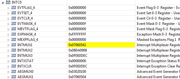
    I'm not sure that INMUX1 register is correctly set  for my pins.

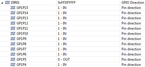
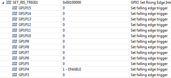
    When i am press the switch SW-1 on GP1[4] pin i have the next:

  • I don't understand what GPIO0_EVENT I must use in my program.
    #define GPIO0_EVENT 65
    This can be a problem ?
  • I solved my problem.

    This is a bug in my code:
     GPIO0_EVENT 65   //              GPIO_B0INT GPIO Bank 0 Interrupt

    It must be so:
     GPIO0_EVENT 41  //               GPIO_B1INT GPIO Bank 1 Interrupt

  • Great! sounds good.
    Thanks for your update.