This thread has been locked.

If you have a related question, please click the "Ask a related question" button in the top right corner. The newly created question will be automatically linked to this question.

SN65LVDS822 for LVDS to TTL

Other Parts Discussed in Thread: SN65LVDS822

TTL Output Frequency is 10MHz, so I can't use normal LVDS TO TTL for this application.

(LCD resolution is 480x272, and PIXEL CLK is 10MHz)

I found SN65LVDS822, but I wonder the LVDS signal is 18bit Color Host to 24bit Color LCD Panel.

My Graphic Controller use 3 channels , whether SN65LVDS822 need 4 channels for 18bit.

can I use SN65LVDS822 for this application?

  • Hello,

        Yes, the SN65LVDS822 can be used for your application, please use this datasheet (pages from 21 to 24) as a reference for your application, and take into account the color bit mapping (SN65LVDS822 datasheet, section 10.1.1).

    Regards,

    Diego.

  • thanks,

    I already found the Color Bit Mapping from SN65LVDS822 datasheet, but I'm afraid that there's no condition for the LVDS signal is 18bit Color Host to 24bit Color LCD Panel.

    My Graphic Controller use 3 channels , whether SN65LVDS822 need 4 channels for 18bit.

    Can you share any Application note about this, or please explain more coherently ?

  • Hello,

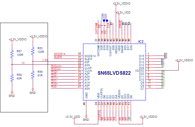
       You can use the 24 bits configuration and use only three input pairs (A0, A1 & A2); meanwhile the fourth differential pair should be polarized to emulate a 1 (or 0), A0p tied to VCM + VID/2 and A0n tied to VCM-VID/2. In order to meet the recommended operating conditions. Then you only have to map the output according to the display.

    Best regards,

    Diego. 

  • thanks for your kind reply.

    At your answer, "A0p tied to VCM + VID/2 and A0n tied to VCM-VID/2." means A3P and A3N , right?

    I think it's just typo, but if not please let me know.

    (cause A0P & A0N should be connected to RX0+ & RX0-.

  • Hi,

    I made  a board according to your recommandation, but I still can't see display.

    please verify my test point is correct.

    LVDS A3P

    VCM : 1.2V

    VID/2 : 0.25V   so 1.45V setting


    LVDS A3N

    VCM :1.2V

    VID/2 : 0.25V so 0.95V setting


    I attach my schematic.

  • Hello,

    I am sorry for my typo, I meant A3P and A3N as you mentioned. Please let me know the status of swap, in order to review the color mapping.

    Regards,
    Diego.
  • Hello,

    Thanks for your help,

    the status of swap is "low" , and I attach my full schematic.

  • Hello,

    Please confirm that mode14 is tied to low, on the schematic seems that it is connected to a pull-up. This pin must be low in order to use all four LVDS channels (so the customer can use only three of them).

    Also please verify that the CLKPOL is configured to work properly with the LVDS transmitter.

    I would like to review the input pinout of the panel connected to J4, just to be sure that there is no color mapping issue.

    Best regards,
    Diego.