This thread has been locked.

If you have a related question, please click the "Ask a related question" button in the top right corner. The newly created question will be automatically linked to this question.

SN65DSI83 producing blank "image"

Other Parts Discussed in Thread: SN65DSI83

Hello!

I'd like to ask you for some advice, what do you think is wrong with our setup.

We are using SN65DSI83 (DSI to LVDS) converter.

Our Panel / Connection specification is:

- 4 DSI data lanes + Clock (all 5 of them are diff. pairs)

- LVDS Panel (1280x800 pix resolution) (attached datasheet and Screenshot of DSI Tuner tool)

- Panel DE is positive polarity driven, HS and VS are both negative polarity driven.

- We are sure that we have working DSI signal on Clock and Data lanes (frequency at about 456MHz)

- We achieved to generate Test patern signal on our LCD (no errors bit set in SN65dsi83 error register (0xE5))

- DSI video has 24bpp, and SN65DSI83 is set to change it in 18bpp video.

- When we turn off Test patern generation feature, we also don't have any error bits set in error register (All bits has zero value) But we still don't have picture on on our panel. LVDS clock looks good, at frequency around 75MHz. What is strange is that signal on Data lane 2 (diff pair) has similar signal as clock lane. On data lane 0 and 1, there is no signal. We have impedance/lenght matched differential pair lanes, with good spacing between them. Hardware shoudn't be problematic.

What do you recommend that we should try and change?


1346.AVD-TT101WX-CN-016-A SP(O).pdf

  • Hello,

    Make sure you have the MIPI inputs driven to LP11(both P and N pairs of all MIPI DSI differential pairs to single ended high ~1.2V) prior to asserting EN pin.

    Could you provide the DSI line time (horizontal sync to the next horizontal sync timing from the APU).   If the line time is different from what is calculated by the tool, this will cause issues.  Even if the DSI source is outputting streams in a burst manner, it is important for the DSI source to fill in the rest of the line time with blanking packets(or LP11) to meet the line time requirement.

    Regards

  • Helo, 

    I'm very thankful for your response. It raised a few more questions, after we try it out and our setup still didn't work. I think that we are really close, and just one or two settings don't match. For the APU we are using Qualcomm's Snapdragon 410, which runs linux kernel 3.10 and Android "on the surface". I've attached file in which are listed commands for setting DSI video output on our main processor. Linux kernel documentation isn't detailed, we are stuck with that. Can you please look at it and say which ones do you think is "right" settings. I also attached pictures taken with oscilloscope. It's bandwidth isn't as high as DSI signals, but some things is still showing.


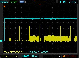
    On the picture above, blue signal show assertion of the SN65DSI83 Enable pin, after reset sequence. Data lanes transits from LP11 state and there is ~7ms delay (From Clock's postitive edge transition to Data's negative transition. This delay is programmable by "qcom,mdss-dsi-init-delay-us=<7000>;")

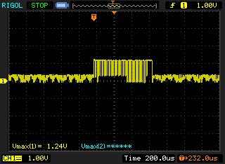
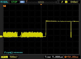
    On picture above, Data lane is shown. It looks like blanking "Pulses" transitions to LP state. Central "block" is not clearly seen because of oscilloscope's low bandwidth.

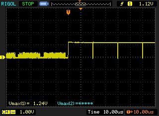
    And on this picture, you can see that "line-time" is always the same (at arround 20us as calculated with DSI Tuner).

    We really need your support. We are developing medical tablet and this is what is holding us back. Attached bellow is "List of properties" that we can set for DSI video output on Qualcomm's APU.

    We would really appreciate if you can give as some advice to help us out.

    Best regards!

    List of possible properties.txt
    ######################################################################################################
    Listed below are some of the properties to set our APU (Qualcomm Snapdragon 410), to output DSI video.
    ######################################################################################################
    
    
    - qcom,mdss-dsi-lp11-init:		Boolean used to enable the DSI clocks and data lanes (low power 11)
    					before issuing hardware reset line.
    - qcom,mdss-dsi-init-delay-us:		Delay in microseconds(us) before performing any DSI activity in lp11
    					mode. This master delay (t_init_delay as per DSI spec) should be sum
    					of DSI internal delay to reach fuctional after power up and minimum
    					delay required by panel to reach functional.
    - qcom,mdss-dsi-h-sync-pulse:		Specifies the pulse mode option for the panel.
    					0 = Don't send hsa/he following vs/ve packet(default)
    					1 = Send hsa/he following vs/ve packet
    - qcom,mdss-dsi-hfp-power-mode:		Boolean to determine DSI lane state during
    					horizontal front porch (HFP) blanking period.
    - qcom,mdss-dsi-hbp-power-mode:		Boolean to determine DSI lane state during
    					horizontal back porch (HBP) blanking period.
    - qcom,mdss-dsi-hsa-power-mode:		Boolean to determine DSI lane state during
    					horizontal sync active (HSA) mode.
    - qcom,mdss-dsi-last-line-interleave	Boolean to determine if last line
    					interleave flag needs to be enabled.
    - qcom,mdss-dsi-bllp-eof-power-mode:	Boolean to determine DSI lane state during
    					blanking low power period (BLLP) EOF mode.
    - qcom,mdss-dsi-bllp-power-mode:	Boolean to determine DSI lane state during
    					blanking low power period (BLLP) mode.
    - qcom,mdss-dsi-traffic-mode:		Specifies the panel traffic mode.
    					"non_burst_sync_pulse" = non burst with sync pulses (default).
    					"non_burst_sync_event" = non burst with sync start event.
    					"burst_mode" = burst mode.
    - qcom,mdss-dsi-pixel-packing:		Specifies if pixel packing is used (in case of RGB666).
    					"tight" = Tight packing (default value).
    					"loose" = Loose packing.
    - qcom,mdss-dsi-lane-0-state:		Boolean that specifies whether data lane 0 is enabled.
    - qcom,mdss-dsi-lane-1-state:		Boolean that specifies whether data lane 1 is enabled.
    - qcom,mdss-dsi-lane-2-state:		Boolean that specifies whether data lane 2 is enabled.
    - qcom,mdss-dsi-lane-3-state:		Boolean that specifies whether data lane 3 is enabled.
    - qcom,mdss-dsi-t-clk-post:		Specifies the byte clock cycles after mode switch.
    					0x03 = default value.
    - qcom,mdss-dsi-t-clk-pre:		Specifies the byte clock cycles before mode switch.
    					0x24 = default value.
    - qcom,mdss-dsi-stream:			Specifies the packet stream to be used.
    					0 = stream 0 (default)
    					1 = stream 1
    - qcom,mdss-dsi-mdp-trigger:		Specifies the trigger mechanism to be used for MDP path.
    					"none" = no trigger
    					"trigger_te" = Tear check signal line used for trigger
    					"trigger_sw" = Triggered by software (default)
    					"trigger_sw_te" = Software trigger and TE
    - qcom,mdss-dsi-dma-trigger:		Specifies the trigger mechanism to be used for DMA path.
    					"none" = no trigger
    					"trigger_te" = Tear check signal line used for trigger
    					"trigger_sw" = Triggered by software (default)
    					"trigger_sw_seof" = Software trigger and start/end of frame trigger.
    					"trigger_sw_te" = Software trigger and TE
    - qcom,mdss-dsi-panel-framerate:	Specifies the frame rate for the panel.
    					60 = 60 frames per second (default)
    - qcom,mdss-dsi-on-command-state:	String that specifies the ctrl state for sending ON commands.
    					"dsi_lp_mode" = DSI low power mode (default)
    					"dsi_hs_mode" = DSI high speed mode
    - qcom,mdss-dsi-off-command-state:	String that specifies the ctrl state for sending OFF commands.
    					"dsi_lp_mode" = DSI low power mode (default)
    					"dsi_hs_mode" = DSI high speed mode
    - qcom,mdss-pan-physical-width-dimension:	Specifies panel physical width in mm which corresponds
    					to the physical width in the framebuffer information.
    - qcom,mdss-pan-physical-height-dimension:	Specifies panel physical height in mm which corresponds
    					to the physical height in the framebuffer information.
    - qcom,mdss-tear-check-disable:		Boolean to disable mdp tear check. Tear check is enabled by default to avoid
    					tearing. Other tear-check properties are ignored if this property is present.
    					The below tear check configuration properties can be individually tuned if
    					tear check is enabled.
    - qcom,mdss-tear-check-sync-cfg-height: Specifies the vertical total number of lines.
    					The default value is 0xfff0.
    - qcom,mdss-tear-check-sync-init-val:	Specifies the init value at which the read pointer gets loaded
    					at vsync edge. The reader pointer refers to the line number of
    					panel buffer that is currently being updated.
    					The default value is panel height.
    - qcom,mdss-tear-check-sync-threshold-start:
    					Allows the first ROI line write to an panel when read pointer is
    					between the range of ROI start line and ROI start line plus this
    					setting.
    					The default value is 4.
    - qcom,mdss-tear-check-sync-threshold-continue:
    					The minimum number of lines the write pointer needs to be
    					above the read pointer so that it is safe to write to the panel.
    					(This check is not done for the first ROI line write of an update)
    					The default value is 4.
    - qcom,mdss-tear-check-start-pos:	Specify the y position from which the start_threshold value is
    					added and write is kicked off if the read pointer falls within that
    					region.
    					The default value is panel height.
    - qcom,mdss-tear-check-rd-ptr-trigger-intr:
    					Specify the read pointer value at which an interrupt has to be
    					generated.
    					The default value is panel height + 1.
    - qcom,mdss-tear-check-frame-rate:	Specify the value to be a real frame rate(fps) x 100 factor to tune the
    					timing of TE simulation with more precision.
    					The default value is 6000 with 60 fps.
    - qcom,partial-update-enabled:		Boolean used to enable partial
    					panel update for command mode panels.
    - qcom,mdss-dsi-horizontal-line-idle:	List of width ranges (EC - SC) in pixels indicating
    					additional idle time in dsi clock cycles that is needed
    					to compensate for smaller line width.
    - qcom,partial-update-roi-merge:	Boolean indicates roi combination is need
    					and function has been provided for dcs
    					2A/2B command.
    - qcom,dcs-cmd-by-left:			Boolean to indicate that dcs command are sent
    					through the left DSI controller only in a dual-dsi configuration
    - qcom,mdss-dsi-rx-eot-ignore:		Boolean used to enable ignoring end of transmission packets.
    - qcom,mdss-dsi-tx-eot-append:		Boolean used to enable appending end of transmission packets.
    - qcom,ulps-enabled:			Boolean to enable support for Ultra Low Power State (ULPS) mode.
    - qcom,suspend-ulps-enabled:		Boolean to enable support for ULPS mode for panels during suspend state.
    - qcom,panel-roi-alignment:		Specifies the panel ROI alignment restrictions on its
    					left, top, width, height alignments and minimum width and
    					height values
    - qcom,esd-check-enabled:		Boolean used to enable ESD recovery feature.
    - qcom,mdss-dsi-panel-status-command:	A byte stream formed by multiple dcs packets based on
    					qcom dsi controller protocol, to read the panel status.
    					This value is used to kick in the ESD recovery.
    					byte 0: dcs data type
    					byte 1: set to indicate this is an individual packet
    						 (no chain)
    					byte 2: virtual channel number
    					byte 3: expect ack from client (dcs read command)
    					byte 4: wait number of specified ms after dcs command
    						 transmitted
    					byte 5, 6: 16 bits length in network byte order
    					byte 7 and beyond: number byte of payload
    - qcom,mdss-dsi-panel-status-command-mode:
    					String that specifies the ctrl state for reading the panel status.
    					"dsi_lp_mode" = DSI low power mode
    					"dsi_hs_mode" = DSI high speed mode
    - qcom,mdss-dsi-panel-status-check-mode:Specifies the panel status check method for ESD recovery.
    					"bta_check" = Uses BTA to check the panel status
    					"reg_read" = Reads panel status register to check the panel status
    					"te_signal_check" = Uses TE signal behaviour to check the panel status
    - qcom,mdss-dsi-panel-status-value:	Specifies the value of the panel status register when the panel is
    					in good state.
    - qcom,dynamic-mode-switch-enabled:		Boolean used to mention whether panel supports
    					dynamic switching from video mode to command mode
    					and vice versa.
    - qcom,video-to-cmd-mode-switch-commands:	List of commands that need to be sent
    					to panel in order to switch from video mode to command mode dynamically.
    					Refer to "qcom,mdss-dsi-on-command" section for adding commands.
    - qcom,cmd-to-video-mode-switch-commands:	List of commands that need to be sent
    					to panel in order to switch from command mode to video mode dynamically.
    					Refer to "qcom,mdss-dsi-on-command" section for adding commands.
    - qcom,mdss-dsi-panel-orientation:	String used to indicate orientation of panel
    					"180" = panel is flipped in both horizontal and vertical directions
    					"hflip" = panel is flipped in horizontal direction
    					"vflip" = panel is flipped in vertical direction
    - qcom,panel-ack-disabled: A boolean property to indicate, whether we need to wait for any ACK from the panel
    			   for any commands that we send.
    - qcom,mdss-dsi-post-init-delay:	Specifies required number of frames to wait so that panel can be functional
    					to show proper display.
    - qcom,mdss-dsi-force-clock-lane-hs:	Boolean to force dsi clock lanes to HS mode always.
    
    ###################### Our current settings  #########################
    &mdss_mdp {
    	dsi_panel_video: qcom,mdss_dsi_panel_video {
    		qcom,mdss-dsi-panel-name = "ADVTT0101 panel";
    		qcom,mdss-dsi-panel-controller = <&mdss_dsi0>;
    		qcom,mdss-dsi-panel-type = "dsi_video_mode";
    		qcom,mdss-dsi-panel-destination = "display_1";
    		qcom,mdss-dsi-panel-framerate = <60>;
    		qcom,mdss-dsi-virtual-channel-id = <0>;
    		qcom,mdss-dsi-stream = <0>;
    		qcom,mdss-dsi-panel-width = <1280>;
    		qcom,mdss-dsi-panel-height = <800>;
    		qcom,mdss-dsi-h-front-porch = <188>;
    		qcom,mdss-dsi-h-back-porch = <52>;
    		qcom,mdss-dsi-h-pulse-width = <8>;
    		qcom,mdss-dsi-h-sync-skew = <0>;
    		qcom,mdss-dsi-v-back-porch = <10>;
    		qcom,mdss-dsi-v-front-porch = <21>;
    		qcom,mdss-dsi-v-pulse-width = <2>;
    		qcom,mdss-dsi-h-left-border = <0>;
    		qcom,mdss-dsi-h-right-border = <0>;
    		qcom,mdss-dsi-v-top-border = <0>;
    		qcom,mdss-dsi-v-bottom-border = <0>;
    		qcom,mdss-dsi-h-active-res = <1280>;
    		qcom,mdss-dsi-v-active-res = <800>;
    		qcom,mdss-dsi-bpp = <24>;
    		qcom,mdss-dsi-underflow-color = <0xff>;
    		qcom,mdss-dsi-border-color = <0>;
    		qcom,mdss-dsi-on-command = [];
    		qcom,mdss-dsi-off-command = [];
    		qcom,mdss-dsi-on-command-state = "dsi_lp_mode";
    		qcom,mdss-dsi-off-command-state = "dsi_hs_mode";
    		qcom,mdss-dsi-h-sync-pulse = <1>;
    		qcom,mdss-dsi-traffic-mode = "non_burst_sync_pulse";
    		qcom,mdss-dsi-lane-map = "lane_map_0123";
    		qcom,mdss-dsi-bllp-eof-power-mode;
    		qcom,mdss-dsi-bllp-power-mode;
    		qcom,mdss-dsi-lane-0-state;
    		qcom,mdss-dsi-lane-1-state;
    		qcom,mdss-dsi-lane-2-state;
    		qcom,mdss-dsi-lane-3-state;
    		qcom,mdss-dsi-panel-timings = [87 1c 12 00 42 44 18 20 17 03 04 00];
    		qcom,mdss-dsi-t-clk-post = <0x04>;
    		qcom,mdss-dsi-t-clk-pre = <0x1b>;
    		qcom,mdss-dsi-bl-min-level = <1>;
    		qcom,mdss-dsi-bl-max-level = <4095>;
    		qcom,mdss-dsi-dma-trigger = "trigger_sw";
    		qcom,mdss-dsi-mdp-trigger = "none";
    		qcom,mdss-dsi-bl-pmic-control-type = "bl_ctrl_wled";
    		qcom,mdss-dsi-force-clock-lane-hs;
    		qcom,mdss-pan-physical-width-dimension = <217>;
    		qcom,mdss-pan-physical-height-dimension = <136>;
    		qcom,mdss-dsi-init-delay-us = <7000>;
    		qcom,mdss-dsi-lp11-init;
    	};
    };

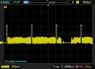
  • I'd like to also  add a few things. On a picture below, you can see transitioning to LP once per frame. 


    And below you can see HFP (188), HSS packet and a HBP (52). And after that last VACT. After that is vertical blaking.

    Status register 0xE5 on SN65DSI83, shows error number 12 (DEC).

    I hope that I wrote good description and that you can give me any advice.

    Best regards!

    Miha B

  • Hello Miha, 

    We are still reviewing the data you have provided. 

    One more thing, can you share the panel datasheet?

    Regards

  • Hello again,

    Attached below is panel datasheet. As I said above, test pattern generation feature is working and we confirmed that everything is OK with the panel.

    We received information about porches value (back &front) and pulse width from the panel's manufacturer. Those values aren't in datasheet. 

    Regards

    6740.AVD-TT101WX-CN-016-A SP(O).pdf

  • The DSI Tuner seems to be configured correctly. The only thing you need to change is the "bits per pixels" field on the Panel Info tab, it should be 24bpp.

    Additionally, provide a register dump of the DSI83 (including the interrupt registers). Is the status register 0xE5 remaining 12 (DEC) even after clearing the interrupts?

    Regards
  • We also tried that. (Changing to 24bpp). But there is no change. Panel has 3 differential data lanes, so it's 18bpp panel. But as I said, we tried both options. We are also periodically reading 0xE5 register and if there is non-zero value, we write 1 to the 0xE5 and "wait" for another one. If we enable test pattern generation, there is zero value and when we try again DSI input, there is value 12 (DEC). We are not using interrupt generation for errors (we are not setting register 0xE1), we are just periodically reading 0xE5. We also tried clock and data equalization (1db and 2db) but that didn't help either.
  • Bit 3 is CHA_LLP_ERR which is set when there are problems decoding SOT (Start Of Text bit/byte sync symbol during the start of a High Speed transmission). If SOT is not decoded correctly, no DSI packets will be received. This indicates fundamental DSI clock/data reception problems. Connectivity and signal quality type problems.
  • We already had concerns about signal quality/integrity. We decided that we would use two separate boards (just for prototyping). On one, there would be APU (Qualcomm's Snapdragon 410) and on the other one, there would be SN65DSI83. Connector used is high speed connector, that is also used on Qualcomm's Development board for CSI (Camera interface). Connector's datasheet is on this link ->

    All data and clock lanes are impedance and length matched.

    We are in process of designing another board, which would have all the components.  Please see picture below of first board and comment if this routing could be the reason for our problem. If you look at the top left of the image, first diff pair on the left side of connector, is for Data Lane 2, then Data Lane 3, Data Lane 1, Data Lane 0 and on the right side is Clock Lanes.

    Thank you for your's comments!

  • We have the same problem with you.Have you solved the problem?
  • Hi! No, we still didn't find the solution. As stated above, we are making new PCB with DSI lanes shorter than 2cm and without connectors. We hope that that will be better. Which processor do you use? Also Q410 from Snapdragon?
  • Hello!

    Can you please give us an opinion regarding our PCB? 

  • Hello Miha, 

    Yes, please post your design files or send them to joel.jimenez@ti.com. 

    Regards