This thread has been locked.

If you have a related question, please click the "Ask a related question" button in the top right corner. The newly created question will be automatically linked to this question.

SN65DSI84: Tooling question

Part Number: SN65DSI84

Hi Sirs,

Sorry to bother you.

As title, we have use SN65DSI84 and download tooling " sllc434c.zip "

We have some questions need check

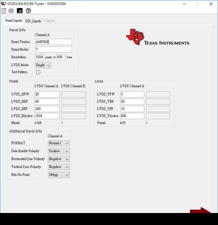
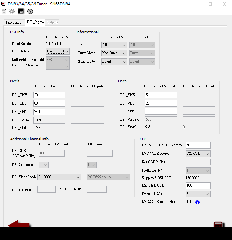
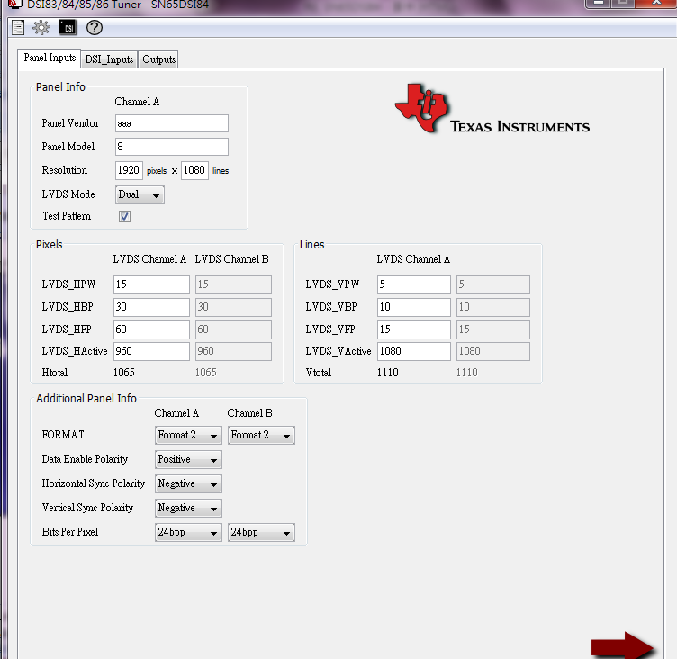
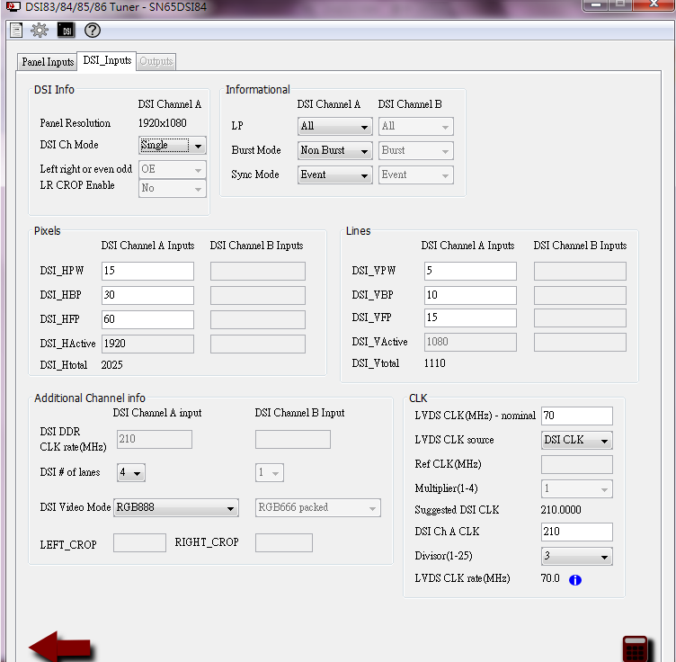
 Our setting as below

We will transfer register data to be our initial code.
There have signal output from MIPI side, also CLK is normally.

But only Y2/CLK had output at DSI84 side, Y0/Y1/Y3 didn't.

The CLK result is same as our setting.

1. We would like to know why no output on Y0/Y1/Y3?

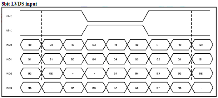
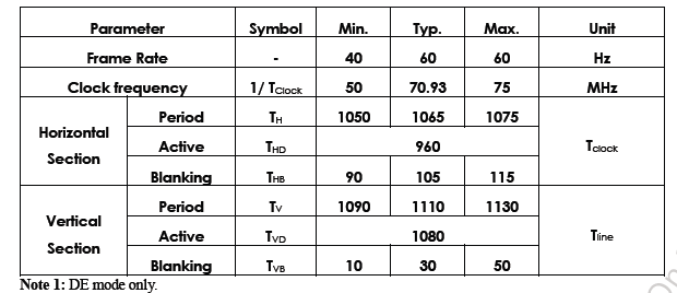
2. Does DSI84 could support LVDS format as below?

If Yes, how to setting? if no, have other solution can share?

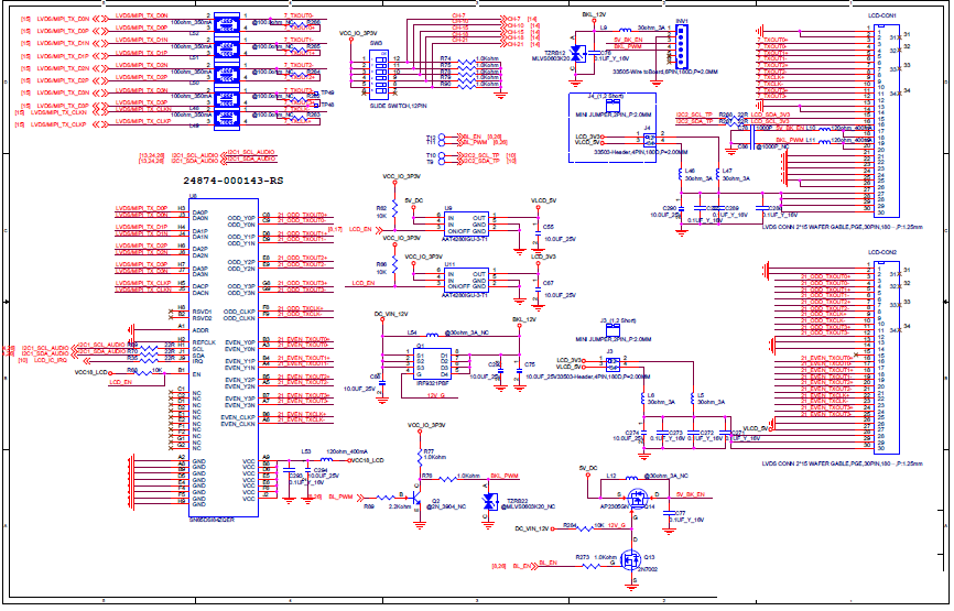
Our schematic:

By the way, DSI84 Test Pattern was pass.

Thanks!!

  • Hello Shu-Chen,

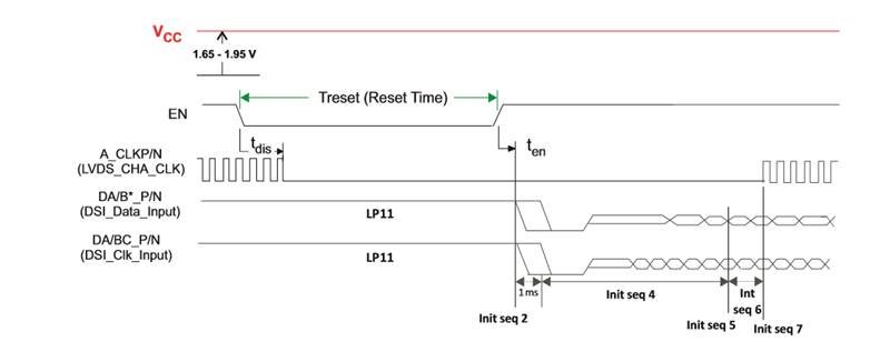
    Make sure you have the MIPI inputs driven to LP11 (both P and N pairs of all MIPI DSI differential pairs to single ended high ~1.2V) prior to asserting EN pin as described in the initialization sequence.

    Please, provide a scope capture showing Vcc, EN, DA0 and DAC at power up.

    Regards,
    Joel

  • Thanks for your reply.

    We still have some question on this tooling.

    Could you help share how to setting dual LVDS application on this tooling?

    Thanks!!

  • Hi Sirs,

    Update our question

    We couldn't turn on the panel when use dual LVDS output

    Step as below

    1. DTSI swtting


                    timing8: timing8 {

                            screen-type = <SCREEN_MIPI>;

                            lvds-format = <LVDS_8BIT_1>;

                            out-face    = <OUT_P888>;

                            clock-frequency = <144000000>;

                            hactive = <1920>;

                            vactive = <1080>;

                            hback-porch = <44>;

                            hfront-porch = <60>;

                            vback-porch = <5>;

                            vfront-porch = <10>;

                            hsync-len = <24>;

                            vsync-len = <5>;

                            hsync-active = <0>;

                            vsync-active = <0>;

                            de-active = <0>;

                            pixelclk-active = <0>;

                            swap-rb = <0>;

                            swap-rg = <0>;

                            swap-gb = <0>;

                            swap-delta = <0>;

                            swap-dummy = <0>;

                    };


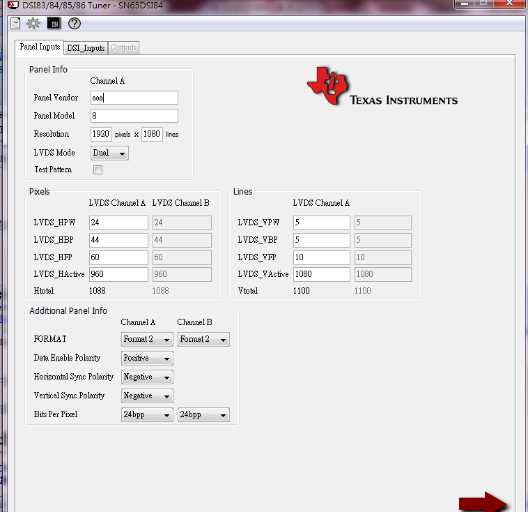
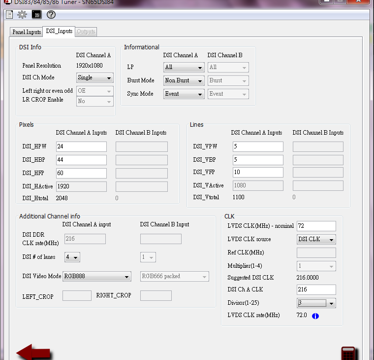
    2. Use dsi tuner tooling to transfer, the pic as below

    Then fill the value

    i2c_reg_write(SN65DSI84_I2C_ADDR, DSI84_SOFT_RESET                  , 0x00);// reg 0x09

            i2c_reg_write(SN65DSI84_I2C_ADDR, DSI84_CORE_PLL                      , 0x05);// reg 0x0a

            i2c_reg_write(SN65DSI84_I2C_ADDR, DSI84_PLL_DIV                         , 0x28);// reg 0x0b

            i2c_reg_write(SN65DSI84_I2C_ADDR, DSI84_PLL_EN                           , 0x00);// reg 0x0d

            i2c_reg_write(SN65DSI84_I2C_ADDR, DSI84_DSI_CFG                         , 0x26);// reg 0x10

            i2c_reg_write(SN65DSI84_I2C_ADDR, DSI84_DSI_EQ                           , 0x00);// reg 0x11

            i2c_reg_write(SN65DSI84_I2C_ADDR, DSI84_CHA_DSI_CLK_RNG               , 0x56);// reg 0x12

            i2c_reg_write(SN65DSI84_I2C_ADDR, 0x13                                          , 0x00);

            i2c_reg_write(SN65DSI84_I2C_ADDR, DSI84_LVDS_MODE                  , 0x6c);// reg 0x18

            i2c_reg_write(SN65DSI84_I2C_ADDR, DSI84_LVDS_SIGN                     , 0x00);// reg 0x19

            i2c_reg_write(SN65DSI84_I2C_ADDR, DSI84_LVDS_TERM                   , 0x03);// reg 0x1a

            i2c_reg_write(SN65DSI84_I2C_ADDR, DSI84_LVDS_CM                               , 0x00);// reg 0x1b

            i2c_reg_write(SN65DSI84_I2C_ADDR, DSI84_CHA_LINE_LEN_LO                , 0x80);// reg 0x20

            i2c_reg_write(SN65DSI84_I2C_ADDR, DSI84_CHA_LINE_LEN_HI         , 0x07);// reg 0x21

            i2c_reg_write(SN65DSI84_I2C_ADDR, 0x22                                          , 0x00);

            i2c_reg_write(SN65DSI84_I2C_ADDR, 0x23                                          , 0x00);

            i2c_reg_write(SN65DSI84_I2C_ADDR, DSI84_CHA_VERT_LINES_LO    , 0x00);// reg 0x24

            i2c_reg_write(SN65DSI84_I2C_ADDR, DSI84_CHA_VERT_LINES_HI     , 0x00);// reg 0x25

            i2c_reg_write(SN65DSI84_I2C_ADDR, DSI84_CHA_VERT_BACKPORCH       , 0x00);// reg 0x36

            i2c_reg_write(SN65DSI84_I2C_ADDR, DSI84_CHA_HORZ_FRONTPORCH   , 0x00);// reg 0x38 

            i2c_reg_write(SN65DSI84_I2C_ADDR, DSI84_CHA_VERT_FRONTPORCH    , 0x00);// reg 0x3a

            i2c_reg_write(SN65DSI84_I2C_ADDR, DSI84_CHA_TEST_PATTERN     , 0x00);// reg 0x3c

            i2c_reg_write(SN65DSI84_I2C_ADDR, 0x26                                          , 0x00);

            i2c_reg_write(SN65DSI84_I2C_ADDR, 0x27                                          , 0x00);

            i2c_reg_write(SN65DSI84_I2C_ADDR, DSI84_CHA_SYNC_DELAY_LO  , 0x20);// reg 0x28

            i2c_reg_write(SN65DSI84_I2C_ADDR, DSI84_CHA_SYNC_DELAY_HI   , 0x00);// reg 0x29

            i2c_reg_write(SN65DSI84_I2C_ADDR, 0x2a                                          , 0x00);

            i2c_reg_write(SN65DSI84_I2C_ADDR, 0x2b                                          , 0x00);

            i2c_reg_write(SN65DSI84_I2C_ADDR, DSI84_CHA_HSYNC_WIDTH_LO       , 0x18);// reg 0x2c

            i2c_reg_write(SN65DSI84_I2C_ADDR, DSI84_CHA_HSYNC_WIDTH_HI        , 0x00);// reg 0x2d

            i2c_reg_write(SN65DSI84_I2C_ADDR, 0x2e                                          , 0x00);

            i2c_reg_write(SN65DSI84_I2C_ADDR, 0x2f                                           , 0x00);

            i2c_reg_write(SN65DSI84_I2C_ADDR, DSI84_CHA_VSYNC_WIDTH_LO       , 0x05);// reg 0x30

            i2c_reg_write(SN65DSI84_I2C_ADDR, DSI84_CHA_VSYNC_WIDTH_HI        , 0x00);// reg 0x31

            i2c_reg_write(SN65DSI84_I2C_ADDR, 0x32                                          , 0x00);

            i2c_reg_write(SN65DSI84_I2C_ADDR, 0x33                                          , 0x00);

            i2c_reg_write(SN65DSI84_I2C_ADDR, DSI84_CHA_HORZ_BACKPORCH      , 0x2c);// reg 0x34

            i2c_reg_write(SN65DSI84_I2C_ADDR, 0x35                                          , 0x00);

            i2c_reg_write(SN65DSI84_I2C_ADDR, 0x37                                          , 0x00);

            i2c_reg_write(SN65DSI84_I2C_ADDR, 0x39                                          , 0x00);

            i2c_reg_write(SN65DSI84_I2C_ADDR, 0x3b                                          , 0x00);

            i2c_reg_write(SN65DSI84_I2C_ADDR, 0x3d                                          , 0x00);

            i2c_reg_write(SN65DSI84_I2C_ADDR, 0x3e                                          , 0x00);

    Follow this step, we could turn on 2 pcs LCD on signal mode, but couldn't on dual mode.

    Our application is Single mipi  to dual LVDS  , even / odd  LVDS to push 1 pcs LCD,  not two LVDS push 2 LCD.

    So, DSI84 can do it? if not, have any others solution can share for us?


  • Hello Shu-Geng

    Were you be able to enable the pattern generator using one display in dual mode?

    Please, share the panel datasheet.

    Regards,
    Joel
  • Hi Sirs,

    Thanks for your reply.

    Q: Were you be able to enable the pattern generator using one display in dual mode?

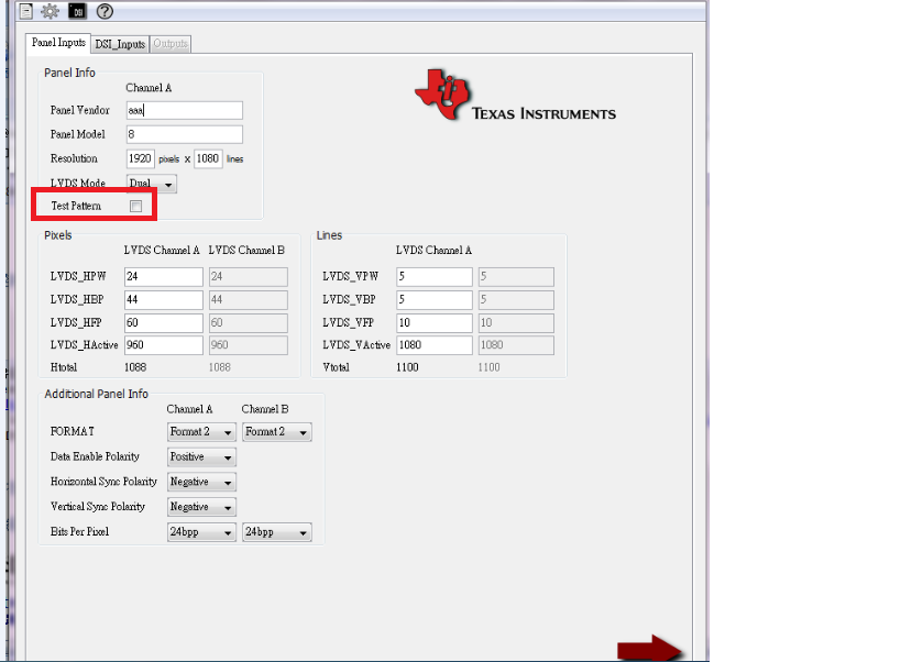
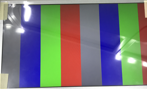
    A: Yes, if the tooling setting Test pattern, we could do it.

  • Hi Sirs,

    But if we don't choose Test pattern, there will fail on Dual mode, but single mode is OK.
    So we guess are we do wrong setting on this tooling?

    By the way, our panel model is G156HTN02.0, G185HAN01.0.
    The panel both are support TWO channel LVDS.

  • Hello,
    Please, read the status registers at offset 0xE1 for both modes (normal and internal pattern).
    Regards
  • Hi Joel,

    Thanks for your reply.

    There have same 0XE1 data between both mode.

    log => sn65DSI84_init_check pass reg = 0xe1, temp = 0x0

    Do we need any setting any enable on  irq ?

    Test pattern pic as below

    Setting step as below

    Then sign in DSI Tuner transfer output value 


    i2c_reg_write(SN65DSI84_I2C_ADDR, DSI84_SOFT_RESET                          , 0x00);// reg 0x09

            i2c_reg_write(SN65DSI84_I2C_ADDR, DSI84_CORE_PLL                              , 0x05);// reg 0x0a

            i2c_reg_write(SN65DSI84_I2C_ADDR, DSI84_PLL_DIV                                 , 0x10);// reg 0x0b

            i2c_reg_write(SN65DSI84_I2C_ADDR, DSI84_PLL_EN                                   , 0x00);// reg 0x0d

            i2c_reg_write(SN65DSI84_I2C_ADDR, DSI84_DSI_CFG                                 , 0x26);// reg 0x10

            i2c_reg_write(SN65DSI84_I2C_ADDR, DSI84_DSI_EQ                                   , 0x00);// reg 0x11

            i2c_reg_write(SN65DSI84_I2C_ADDR, DSI84_CHA_DSI_CLK_RNG               , 0x2a);// reg 0x12

            i2c_reg_write(SN65DSI84_I2C_ADDR, 0x13                                                  , 0x00);

            i2c_reg_write(SN65DSI84_I2C_ADDR, DSI84_LVDS_MODE                          , 0x6c);// reg 0x18

            i2c_reg_write(SN65DSI84_I2C_ADDR, DSI84_LVDS_SIGN                             , 0x00);// reg 0x19

            i2c_reg_write(SN65DSI84_I2C_ADDR, DSI84_LVDS_TERM                           , 0x03);// reg 0x1a

            i2c_reg_write(SN65DSI84_I2C_ADDR, DSI84_LVDS_CM                               , 0x00);// reg 0x1b

            i2c_reg_write(SN65DSI84_I2C_ADDR, DSI84_CHA_LINE_LEN_LO                , 0xc0);// reg 0x20

            i2c_reg_write(SN65DSI84_I2C_ADDR, DSI84_CHA_LINE_LEN_HI                 , 0x03);// reg 0x21

            i2c_reg_write(SN65DSI84_I2C_ADDR, 0x22                                                  , 0x00);

            i2c_reg_write(SN65DSI84_I2C_ADDR, 0x23                                                  , 0x00);

            i2c_reg_write(SN65DSI84_I2C_ADDR, DSI84_CHA_VERT_LINES_LO            , 0x38);// reg 0x24

            i2c_reg_write(SN65DSI84_I2C_ADDR, DSI84_CHA_VERT_LINES_HI             , 0x04);// reg 0x25

            i2c_reg_write(SN65DSI84_I2C_ADDR, DSI84_CHA_VERT_BACKPORCH       , 0x0a);// reg 0x36

            i2c_reg_write(SN65DSI84_I2C_ADDR, DSI84_CHA_HORZ_FRONTPORCH   , 0x3c);// reg 0x38 

            i2c_reg_write(SN65DSI84_I2C_ADDR, DSI84_CHA_VERT_FRONTPORCH    , 0x0f);// reg 0x3a

            i2c_reg_write(SN65DSI84_I2C_ADDR, DSI84_CHA_TEST_PATTERN             , 0x10);// reg 0x3c

            i2c_reg_write(SN65DSI84_I2C_ADDR, 0x26                                                  , 0x00);

            i2c_reg_write(SN65DSI84_I2C_ADDR, 0x27                                                  , 0x00);

            i2c_reg_write(SN65DSI84_I2C_ADDR, DSI84_CHA_SYNC_DELAY_LO          , 0xe1);// reg 0x28

            i2c_reg_write(SN65DSI84_I2C_ADDR, DSI84_CHA_SYNC_DELAY_HI           , 0x03);// reg 0x29

            i2c_reg_write(SN65DSI84_I2C_ADDR, 0x2a                                                  , 0x00);

            i2c_reg_write(SN65DSI84_I2C_ADDR, 0x2b                                                  , 0x00);

            i2c_reg_write(SN65DSI84_I2C_ADDR, DSI84_CHA_HSYNC_WIDTH_LO       , 0x0f);// reg 0x2c

            i2c_reg_write(SN65DSI84_I2C_ADDR, DSI84_CHA_HSYNC_WIDTH_HI        , 0x00);// reg 0x2d

            i2c_reg_write(SN65DSI84_I2C_ADDR, 0x2e                                                  , 0x00);

            i2c_reg_write(SN65DSI84_I2C_ADDR, 0x2f                                                   , 0x00);

            i2c_reg_write(SN65DSI84_I2C_ADDR, DSI84_CHA_VSYNC_WIDTH_LO       , 0x05);// reg 0x30

            i2c_reg_write(SN65DSI84_I2C_ADDR, DSI84_CHA_VSYNC_WIDTH_HI        , 0x00);// reg 0x31

            i2c_reg_write(SN65DSI84_I2C_ADDR, 0x32                                                  , 0x00);

            i2c_reg_write(SN65DSI84_I2C_ADDR, 0x33                                                  , 0x00);

            i2c_reg_write(SN65DSI84_I2C_ADDR, DSI84_CHA_HORZ_BACKPORCH      , 0x1e);// reg 0x34

            i2c_reg_write(SN65DSI84_I2C_ADDR, 0x35                                                  , 0x00);

            i2c_reg_write(SN65DSI84_I2C_ADDR, 0x37                                                  , 0x00);

            i2c_reg_write(SN65DSI84_I2C_ADDR, 0x39                                                  , 0x00);

            i2c_reg_write(SN65DSI84_I2C_ADDR, 0x3b                                                  , 0x00);

            i2c_reg_write(SN65DSI84_I2C_ADDR, 0x3d                                                  , 0x00);

            i2c_reg_write(SN65DSI84_I2C_ADDR, 0x3e                                                  , 0x00);


    /* about mipi */

                    disp_mipi_init: mipi_dsi_init{

                                            compatible = "rockchip,mipi_dsi_init";

                                            rockchip,screen_init       = <0>;

                                            rockchip,dsi_lane            = <4>;

                                            rockchip,dsi_hs_clk         = <420>;

                                            rockchip,mipi_dsi_num  = <1>;

                    };

                    disp_mipi_power_ctr: mipi_power_ctr {

                                            compatible = "rockchip,mipi_power_ctr";

                                            pinctrl-names = "default";

                                            pinctrl-0 = <&gpio0_c6 &gpio1_d4>;//LCD_EN , LCD_IC_IRQ

                                            /*mipi_lcd_rst:mipi_lcd_rst{

                                                            compatible = "rockchip,lcd_rst";

                                                            rockchip,gpios = <&gpio1 GPIO_D4 GPIO_ACTIVE_HIGH>;

                                                            rockchip,delay = <10>;

                                            };*/

                                            mipi_lcd_en:mipi_lcd_en {

                                                            compatible = "rockchip,lcd_en";

                                                            rockchip,gpios = <&gpio0 GPIO_C6 GPIO_ACTIVE_HIGH>;

                                                            rockchip,delay = <10>;

                                            };

                    };

                    disp_mipi_init_cmds: screen-on-cmds {

                                            compatible = "rockchip,screen-on-cmds";

                                            rockchip,cmd_debug = <0>;

                    };


            disp_timings: display-timings {

                    native-mode = <&timing0>;

            timing0: timing0 {

                            screen-type = <SCREEN_MIPI>;

                            lvds-format = <LVDS_8BIT_1>;

                            out-face    = <OUT_P888>;

                            clock-frequency = <140000000>;

                            hactive = <1920>;

                            vactive = <1080>;

                            hback-porch = <30>;

                            hfront-porch = <60>;

                            vback-porch = <10>;

                            vfront-porch = <15>;

                            hsync-len = <15>;

                            vsync-len = <5>;

                            hsync-active = <0>;

                            vsync-active = <0>;

                            de-active = <0>;

                            pixelclk-active = <0>;

                            swap-rb = <0>;

                            swap-rg = <0>;

                            swap-gb = <0>;

                            swap-delta = <0>;

                            swap-dummy = <0>;

                    };


  • Hi Sirs,
    Sorry for pushed.
    Any idea on this case?
  • Hello Shu-Cheng LIN ,
    Sorry my bad, I meant to refer to the offset 0xE5. Please, read this register then clear it by writing 0xFF and then read it again. Does any flag keep set after clearing it?
    Regards
  • Hello Shu-Cheng LIN,
    Sorry for the delay in our response, we are still analYzing your case. It would help if you can send a complete register dump of the device including the 0XE5 and 0XE6 registers.
    Regards
  • Hi Sirs,

    Please refer as below

    ==> sn65DSI84 reg = 0x9, data = 0x0

    ==> sn65DSI84 reg = 0xa, data = 0x5

    ==> sn65DSI84 reg = 0xb, data = 0x10

    ==> sn65DSI84 reg = 0xd, data = 0x1

    ==> sn65DSI84 reg = 0x10, data = 0x26

    ==> sn65DSI84 reg = 0x11, data = 0x0

    ==> sn65DSI84 reg = 0x12, data = 0x2a

    ==> sn65DSI84 reg = 0x13, data = 0x0

    ==> sn65DSI84 reg = 0x18, data = 0x6c

    ==> sn65DSI84 reg = 0x19, data = 0x0

    ==> sn65DSI84 reg = 0x1a, data = 0x3

    ==> sn65DSI84 reg = 0x1b, data = 0x0

    ==> sn65DSI84 reg = 0x20, data = 0x80

    ==> sn65DSI84 reg = 0x21, data = 0x7

    ==> sn65DSI84 reg = 0x22, data = 0x0

    ==> sn65DSI84 reg = 0x23, data = 0x0

    ==> sn65DSI84 reg = 0x24, data = 0x0

    ==> sn65DSI84 reg = 0x25, data = 0x0

    ==> sn65DSI84 reg = 0x36, data = 0x0

    ==> sn65DSI84 reg = 0x38, data = 0x0

    ==> sn65DSI84 reg = 0x3a, data = 0x0

    ==> sn65DSI84 reg = 0x3c, data = 0x0

    ==> sn65DSI84 reg = 0x26, data = 0x0

    ==> sn65DSI84 reg = 0x27, data = 0x0

    ==> sn65DSI84 reg = 0x28, data = 0xe1

    ==> sn65DSI84 reg = 0x29, data = 0x3

    ==> sn65DSI84 reg = 0x2a, data = 0x0

    ==> sn65DSI84 reg = 0x2b, data = 0x0

    ==> sn65DSI84 reg = 0x2c, data = 0xf

    ==> sn65DSI84 reg = 0x2d, data = 0x0

    ==> sn65DSI84 reg = 0x2e, data = 0x0

    ==> sn65DSI84 reg = 0x2f, data = 0x0

    ==> sn65DSI84 reg = 0x30, data = 0x5

    ==> sn65DSI84 reg = 0x31, data = 0x0

    ==> sn65DSI84 reg = 0x32, data = 0x0

    ==> sn65DSI84 reg = 0x33, data = 0x0

    ==> sn65DSI84 reg = 0x34, data = 0x1e

    ==> sn65DSI84 reg = 0x35, data = 0x0

    ==> sn65DSI84 reg = 0x37, data = 0x0

    ==> sn65DSI84 reg = 0x39, data = 0x0

    ==> sn65DSI84 reg = 0x3b, data = 0x0

    ==> sn65DSI84 reg = 0x3d, data = 0x0

    ==> sn65DSI84 reg = 0x3e, data = 0x0


    ==> sn65DSI84 reg = 0xe5, data = 0x1

    ==> sn65DSI84 reg = 0xe6, data = 0x0

  • Hello, 

    We are checking your register configuration to detect any error. In the meantime, please confirm you are following the power-up sequence as stated in the device datasheet. 

    It is highly important to follow the init sequence as stated in the device datasheet. If DSI interface is driven to illegal states/protocol by the host, the SN65DSI8x may get into undesirable states.

    FYI..

    It is required by the MIPI spec for the host to drive DSI outputs to LP11 prior to the transition to the HS mode. The initialization/transition sequence requirement is per the MIPI DPHY version 1.0.0 (Section 6.11) and DSI version 1.02.0 (Section 5.7) specification requirements.

    If possible, send scope captures showing EN pin, DSIA, DSI CLK and VCC at power up.