This thread has been locked.

If you have a related question, please click the "Ask a related question" button in the top right corner. The newly created question will be automatically linked to this question.

SN65DP159: About SN65DP159

Part Number: SN65DP159

Hi dear supporting team,

when customer using SN65DP159 displayport SINK, they set DP159 in retimer mode, but in TP1 stage, they will find PLL LOCK_COMPLETE is not set to 1, and

BERT_CNT[7:0] reg(BERT error count. Lane 0) is not 0, could you pls help suggest how to do trouble shooting?tks!

  • Vera,

    We are looking into your issue and will get back to you as soon as possible.
  • hi Barton,

    tks for the reply! customer is pushing for the help, could you help? tks!

  • Vera,

    Under what conditions do you see this occur? What is the data rate when you see this error? Are you using custom software for design? Could you give a block diagram of the system? 

  • hi Malik,
    thanks for the reply!
    for your questions:
    Under what conditions do you see this occur?--dp159 connect to xilinx DPRXSS IP core,dp source is from PC ;
    What is the data rate when you see this error?--the data rate os 1.62Gbps;
    Are you using custom software for design? --they are using the interface provided by xilinx for visiting DP159, the reg setting process is the same with TI slla358.pdf ref doc(and they are assure that DP159 could be visit through I2c interface)
    Could you give a block diagram of the system?-- dp source->dp159->xilinx video phy->xilinx dprxss
    pls help check anything that could be debugged? tks!
  • Vera,

    Have you tried operating your setup at higher data rates? Is it only this data rate that does not work? It seems that the TP1 signal is weak, potentially having too much jitter or small VOD. You should confirm that VOD is being changed automatically by the xilinx system. Also minimize the distance between the DP source and dp159 in order to minimize potential SI issues. For HW, debug you could probe Refclk_out to see if this clock has the appropriate frequency, please see 4.5 REFCLK_OUT in slla358.pdf.

  • We are supporting this thread internally.
  • hi Malik,
    thank you for your support!
    the originally issue is closed now, the root cause is found to be 0x2F setting and doing to much print when debug, when they delete the print during debug then the training is ok.
    here are two questions left:
    1. they can training sucessfully with the same 2m thick cable in both their brd and XILINX Brd with DP signal, while if they use 1.5m and thinner cable, Xilinx brd can always training sucessfully, while in their brd, there will be some failure rate, is it due to the equalization setting at the receiver, what do you think?

    2. now in their product, dp rxss is set as 1.62Gbps, 4 lane, but after training done, the result is 1.62Gbps 2-lane, with the same source and cable, in Xilinx BRD KC705 , it will still be 1.62Gbps, 4 lane, what's the possiible issue here? tks!
  • Vera,

    Here are some comments to your questions:

    1. The thinner cable may have a bad insertion loss profile. The EQ setting should be increased to try an minimize failure rate.

    2. This seems to be SI related issues here increasing EQ settings may help with this. 

  • hi Malik,

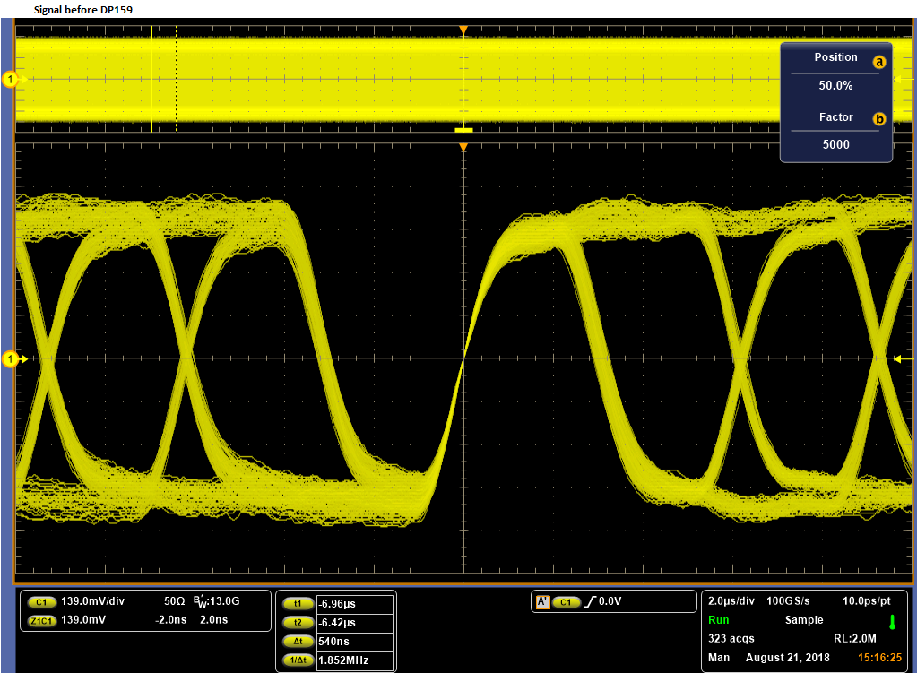
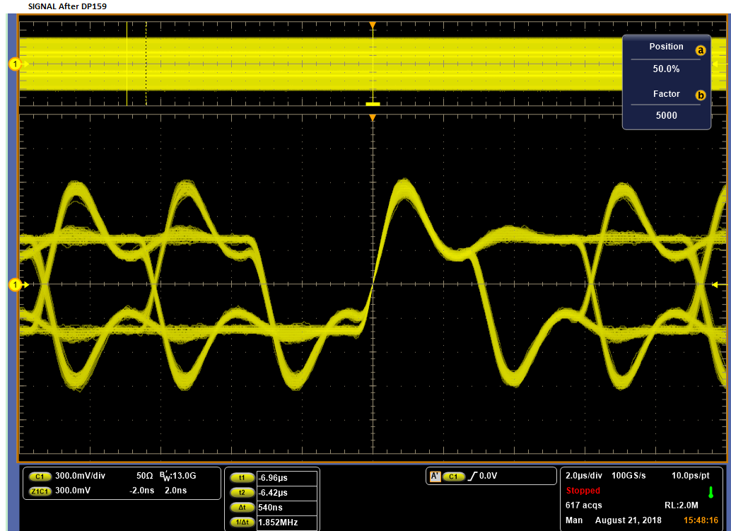
    for the 2nd issue,  (4 lane change to 2 lane), customer test the jitter before and after DP159, the result is as attached, and waveform as below, pls help check whether they need change the EQ setting.  jitter result.7z

  • Vera

    Looking at the signal output of DP159, it looks like the signal is over-compensated. What are your EQ and de-emphasis/pre-emphasis settings? I would try to reduce them first.

    How do you implement your AUX bus?

    Thanks
    David
  • hi David,

    double checked with customer, they did not set any eq in the link: 0ch bit [1,0] is 00, and 0dh bit [5;3]  is 000,  AUX_src is used as CLK output.  so what's the possible cause for the lane  number change and the over compensate? tks!

  • Vera

    For the output measurement of DP159, where do they measure the waveform?

    If they change bit [1:0] of address 0x0Ch and bit [5:3] of address 0x0Dh, are they seeing changes in the waveform? I want to make sure DP159 is being properly controlled.

    Without looking at the link training log file, I can only speculate that when link training failed at 4 lanes, the source changed the lane count down to 2, and start the link training again.

    Any chance you can send me the schematic in .pdf and layout in Allegro format?

    Thanks

    David 

  • hi David,
    will send you the information at helpme. tks!
  • hi David,
    AUX bus is used for recvered clk out and send for FPGA as reference. the EQ setting and pre-emphasis is all default value. (i.e. no equalization), while the output waveform seems be over -compensated.
    customer test the output at both DP159 output and FPGA input, the waveform is similar.
    they found when changind the reg of 0x0c and 0x0d to set the eq, there is no changing in the waveform, and the read out of 0x0c bit [1:0] is always 0, nothing changed.
    so is there other reg need be set for setting the eq? what's the possible cause for the over -compensation? tks!
  • Vera

    So the issue is resolved and we can close this?

    Thanks
    David
  • Hi David,

    No , the 4 lane to 2 lane issue is closed, while the over compensation issue is not yet. Pls help check why the 0x 0c and 0x0d seems could not control the eq well as descript in my previous email. Tks !

  • Vera

    1. Customer is using DP159 as a DP retimer, so EQ programming is not done through Page 0 register. EQ programming is done through Page 1 register. Please refer to app note SLLA358.pdf, section 4 on how to access Page 1 and TX and RX configuration.

    {0xFF, 0x01} , // Select Page 1
    //CONFIGURE PLL BLOCK
    {0x00, 0x02} , //Enable Bandgap.
    {0x04, 0x80} , //PLL_FBDIV[7:0]
    {0x05, 0x00} , //PLL_FBDIV[10:8]
    {0x08, 0x00} ,
    {0x0D, 0x02} , //Select LN0 for clock.
    {0x0E, 0x03} , //CDR_CONFIG[4:0]. FIXED, LN0.
    {0x01, 0x01} , //CP_EN is PLL mode
    {0x02, 0x3F} , //CP_CURRENT is high.
    {0x0B, 0x33} , //Loop Filter to 8K.
    {0xA1, 0x02} , //Allows for Override of PLL settings.
    {0xA4, 0x02} , //Allows for Override of PLL settings.
    //CONFIGURE TX BLOCK
    {0x10, 0xF0} , //ENTX for all four lanes (disable)
    {0x11, 0x30} , //TX_RATE is Full Rate, TX_TERM = 75 to 150 , TX_INVPAIR = None
    {0x14, 0x00} , //HDMI_TWPST1 is 0dB pre-emphasis
    {0x12, 0x03} , //SLEW_CTRL is Normal, SWING is 600mV.
    {0x13, 0xFF} , //FIR_UPD. Load TX settings
    {0x13, 0x00} ,
    //CONFIGURE RX BLOCK
    {0x30, 0xE0} , //Disable Receivers except lane 0
    {0x32, 0x00} , //PD_RXINT
    {0x31, 0x00} , //RX_RATE is Full
    {0x4D, 0x08} , //EQFTC = 0 and EQLEV = 8
    {0x4C, 0x01} , //Enable Fixed EQ
    {0x34, 0x01} , //Enable Offset correction
    {0x32, 0xF0} , //Load RX settings.
    {0x32, 0x00} ,
    {0x33, 0xF0} , //Load EQ settings.

    2. It is better to change the TX SWING level from min to max level as it is easier to be observed on the scope to make sure you have full I2C control over RX and TX control register.

    3. The over-compensation you saw in the measured waveform could come from reflection. The way to measure the DisplayPort signal is to measure the signal at the end of transmission line. So the ideal way to measure the DP signal would be
    a. Remove the AC coupling cap between DP159 and FPGA (break the link between DP159 and FPGA so the measurement is not impacted by possible reflection)
    b. Have the AC coupling cap on the scope, and assume signal line is being terminated inside the scope, do the measurement

    Thanks
    David