This thread has been locked.

If you have a related question, please click the "Ask a related question" button in the top right corner. The newly created question will be automatically linked to this question.

TCA9509RVH - Dimension of pin1

Guru 19775 points

Hi Team,

Could you please tell me the dimension of pin1 of TCA9509RVH ?

I believe the dimension is as below.

(1) 0.25 to 0.35mm
(2) 0.15 to 0.25mm
(3) 0.25 to 0.35mm
(4) 0.125 to 0.175mm

Please correct me if my understanding above is incorrect.

I also have one more question.

What is the worst length for (1) - (2) ? I could calculate as 0.25-0.25 = 0mm.
What would be the minimum length for (1) - (2) ?

Best Regards,
Kawai

  • Kawai,

    Your interpretation of these lengths is correct, and as a result, theoretically the minimum of (1) - (2) would be 0mm.

    I am forwarding this question to the packaging team who can confirm, but my assumption is the process determines whether all pads are approaching the min or all pads are approaching the max.

    By this logic, (1) - (2) would always be 0.1mm.

    This is similar to the concept that resistors on an IC have a tolerance but the proportion of all the resistances is always well identical regardless of whether the resistances are all on the higher due to process changes or all on the lower end due to process changes.

  • Hello Brian-san,

    Thank you very much for the information, I understood your logic.

    First, I will answer the length of (1) to (4) to our customer. Could you please tell me the answer of the packaging team when it is confirmed ?

    Best Regards,
    Kawai

  • Hello Brian, Kawai-san,

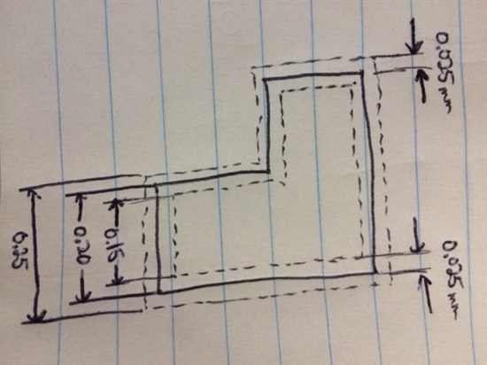
    The dimensions you suggest for the modified pin 1 are essentially correct, with one minor exception. The range (tolerance) of (4) does not cut in half, so it has a formal range of 0.1-0.2 mm.  To help you visualize, a minimum feature size and shape can be generated by drawing a border inset by .025 mm all the way around, and a maximum feature size by a border outboard by .025 all of the way around.  Of course, the actual process normally runs much tighter than this.

    With respect to the question about (1) - (2), again you are essentially correct, the drawing allows a difference of zero but it is extremely unlikely.  You are correct that the exposed features tend to vary in the same direction, all smaller or all larger.  But the sources of variation are not completely consistent so it would be better to say (1) - (2) will generally be pretty close to 0.1 mm and the pin 1 feature will alway have its recognizable shape (which is the whole point of making in non-rectangular). 

    Regards,
    Jeff Holloway
    Analog Packaging 

  • Hi Jeff-san,

    I apologize for my delay.

    Thank you very much for the information. I understood that the length for (4) is 0.1mm to 0.2mm. However, I could not understand the information below. Could you please give me an explanation in other words ?

    >To help you visualize, a minimum feature size and shape can be generated by drawing a border inset by .025 mm all the way around, and a maximum feature size by a border outboard by .025 all of the way around.

    I also have a request to correct the figure of QFN package dimension in the next datasheet update timimg, because, all user would read the length for (4) as half the length of (3).

    * I believe there would be no problem as long as the user  design is based on "Example Board Layout" in the datasheet page 18.

    Best Regards,
    Kawai

  • Kawai,

    To help visualize Jeff's explanation, I have attached a rough sketch using the 0.025mm inset and outside border to show how 0.2mm in dimension (2) can grow to 0.25mm or shrink to 0.15mm 

    I agree that this does not explain the (4) has a formal length of 0.1-0.2mm, and that in the future it may be beneficial to call out this dimension so other customers do not assume that it (4) is (3) cut in half.

    On the other hand, pin 1 only has different dimensions so that it can be visually distinguished from pins 3, 5, and 7. And because pin 1 will always have this shape as in the attached drawing, any customer following the "Example Board Layout" will have no problems with their PCB.