This thread has been locked.

If you have a related question, please click the "Ask a related question" button in the top right corner. The newly created question will be automatically linked to this question.

PCA9306 Sequencing Question

Other Parts Discussed in Thread: PCA9306

Ihave a customer using the PCA9306 as a level translator.  They want to know if there are any sequencing requirements beteewn the VREF pins.


They expect there to be a condition where VREF2 will be at 3.3V for a long time before VREF1 comes up to 1.8V.

  • Hello Max,

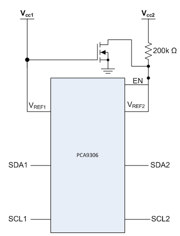
    We suggest that VREF1 come up before VREF2. Due to the fact that the EN pin and VREF2 pin are connected together and then are pulled up to VCC through a 200k ohm resistor, this allows the EN pin to go low when VREF2 is low, disabling the ports and putting them into HighZ. If VREF2 is high and VREF1 is low, this is not necessarily true and the ports will likely be in some intermediate state (not quite high Z but not completely on).

    I estimate that you'll see ~75mV at SDA1 if SDA2 is high, which shouldn't violate any VIH specs, but you will likely have more than the 10 uA of current which the I2C allows as a maximum for leakage.

    If you can't live with this, I would suggest that you use a NMOS to pull the node low if VREF1 goes low, see my sketch below. This can also be accomplished with a regular MOSFET by putting an inverter in between VCC1 and the gate of the FET, of course the inverter needs to be powered.

  • Jonathan,

    My customer also had the same question and I informed that VREF1 should come up prior to VREF2. And then the customer asked another question that how long interval is required between coming up the VREF1 and VREF2.
    If you can show a timing chart of the power up sequencing, it would be very helpful for us.

    Thanks in advance.

  • Wasa-san,

    There is no specific timing. VREF1 and VREF2 may come up at the same time or VREF1 may come up first. There is no digital logic that can get latched, so timing is not critical. Just know that if your EN and VREF2 pins are connected together and then connected to VDU through a 200k pull up, that translation will not happen until the VDU rail ramps up, because the EN pin will be low with VREF2.

    THe reason you should not turn VDU on before VREF1 is because if VREF1 is low, and VDU is high, then the EN pin will get triggered, which will cause the low signal on the VREF1 side to propagate to the VREF2 side, latching your I2C bus low until VREF1 comes up.

    The EN pin allows for translation, but must be connected directly to the VREF2 pin for this to happen. You must then connect those pins to VDU through a pull up resistor of 200k.
  • Jonathan,

    You mean VREF1 should be equal to or higher than VREF2, right?
    Let's say VREF1 = 1.8V and VREF2 = 3.3V. In this case VREF2 should be over VREF1 during coming up.
    So what I like to know is until when we should ensure that the VREF1 should be higher than VREF2. In other words, how much voltage is required in order to enable VREF1 side circuit?
  • Almost, you have it backwards. VREF2 in should be at a higher voltage than VREF1 pin.
    The reason why we state that VREF1 < VREF2 in the datasheet is for when the device is translating, as this will bias the EN pin to allow translation. If VREF1 is high and VREF2 is low, it should pull the EN pin low, putting the device in a high impedance state.


    Allow me to go over this with a designer as there are multiple aspects to check.