This thread has been locked.

If you have a related question, please click the "Ask a related question" button in the top right corner. The newly created question will be automatically linked to this question.

I2C bidirectional level-translator to a bigger or lower reference

Other Parts Discussed in Thread: PCA9306

Hi everybody,


I need to connect an I2C master device biased at 3.3 V to an I2C slave device that can be biased from 2.3 to 5.5 V.

1.- Is it any level translator that I can use? I only found level translators that require that one of the reference voltage is always bigger that the other.

2.- If there is no simple chip to do that, Is it possible to use some thing like this (VDD ranges from 2.3 to 5.5 V)?

Thank you in advance

Best regards GuiX

  • Hello GuiX,

    Thanks for the question.

    Your idea is a clever approach to the problem. I would say that so long as as you maintain the VREF1 side being <= Vref2 - 0.6V (which is looks like you took into consideration already), you should be ok.

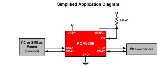
    One thing I would like to note, is that the EN and VREF2 pins are supposed to be shorted together, and then tied to the power rail through a 200k resistor. If you tie VREF2 directly to a power rail, you will encounter translation issues. The VREF2 pin is used to bias the EN pin with the help of the 200k pull-up resistor.

    Another concern you will want to keep in mind, is that when any slave device transmits a 0 on any side of the bus, the TOTAL current through all pull-up resistors will have to be sunk by the transmitting device. IE, in your example, let's say that your variable power rail is at 5V.

    If a 0 is transmitted at P20/19 or P30/29 (or even P25/24, even though you don't have a slave at this intermediate node), it would have to sink the total of:

    5/4.7k = 1.064 mA

    1.65/4.7k = 0.351 mA

    3.3/4.7k = 0.702 mA

    total = 2.117 mA.

    You can see why you will want to try to keep the pull-up resistance as high as you can to help minimize this current.

    Another option is to isolate both sides of the bus by using a buffered translator in place of 1 of the PCA9306 devices (or both if you wish to eliminate any of this between voltage domain current.

    Also I'm kind of curious what your application is that requires a large range on the VDD rail.

  • Hi Jonathan,

    Thank you very much for your support. I incorporated your suggestions:

    The pull-up resistors are tentative values. I will do some experiments to seek the higher value that ensures proper communication.


    Please, let me know if you see some thing wrong.

    Regards

    GuiX

  • GuiX,

    Your EN and VREF2 pins are now properly connected. Everything looks good to go, other than the pull-up resistors, which you will experiment with. I would start with 10k ohms as your base line for those resistors shown, and work from there.
  • Hi every one,

    The board is assembled and I am testing it. It works fine for I2C at 400 kHz but when I measure the 1.65 V signal connected to VREF1 at U8 and U9 I read 3.6 V when VDD = 3.3 V and  VDD_USB = 5 V. Removing U8 and U9 the signal recovers the 1.65 V. There are not any other circuitry connected to the 1.65 V regulator.

    I can not explain this. Is there any one that have any clue about this issues?

    This is the circuit:

    Any hint will be really apreciated.

  • Hello GuiX,

    That is interesting. Your schematic that you have is correct. There is one cause that comes to mind.

    Your power supply (TPS769xx) is unable to sink any current. If it cannot sink any current, then you will see a higher voltage. The reason for this is that current flows from the VREF2 pin into the VREF1 pin (which would flow into the power supply). If your power supply cannot handle sinking current, then the voltage will raise.

    To verify this, try putting a resistor from the 1.65V rail to ground. This will allow the extra voltage to be bled off if your power supply cannot handle it.

    I'm not sure what your power supply's current rating is, but my estimations would say to start with any resistor value at ~40k ohms or lower.
  • Yes !!! 10K Ohm did the trick.
    I did not realize that the feedback resistor divider only consumes 7 uA.
    Nicest approach will be to resize the feedback resistor divider to consume around 200 uA.

    Thanks
  • Hi,

    Why we are using 200K resistor in biasing of EN and VREF. With 5uA requirement of IC there will be 1V drop across that.
  • Gentle Reminder!!
    Please reply.
  • Hi Saurabh,
    The 200k resistor between VREF2 and EN helps minimize the biasing circuit current for the PCA9306 translator. You can connect a small resistor too (like 50k or 100k), but that would have larger current consumption compared to 200k case.

    Please let us know if you have any questions.

    Thanks,
    Rajan