This thread has been locked.

If you have a related question, please click the "Ask a related question" button in the top right corner. The newly created question will be automatically linked to this question.

P82B96 I2C communication over 25 meter CAT6 cable

Other Parts Discussed in Thread: P82B96

Hi Community,

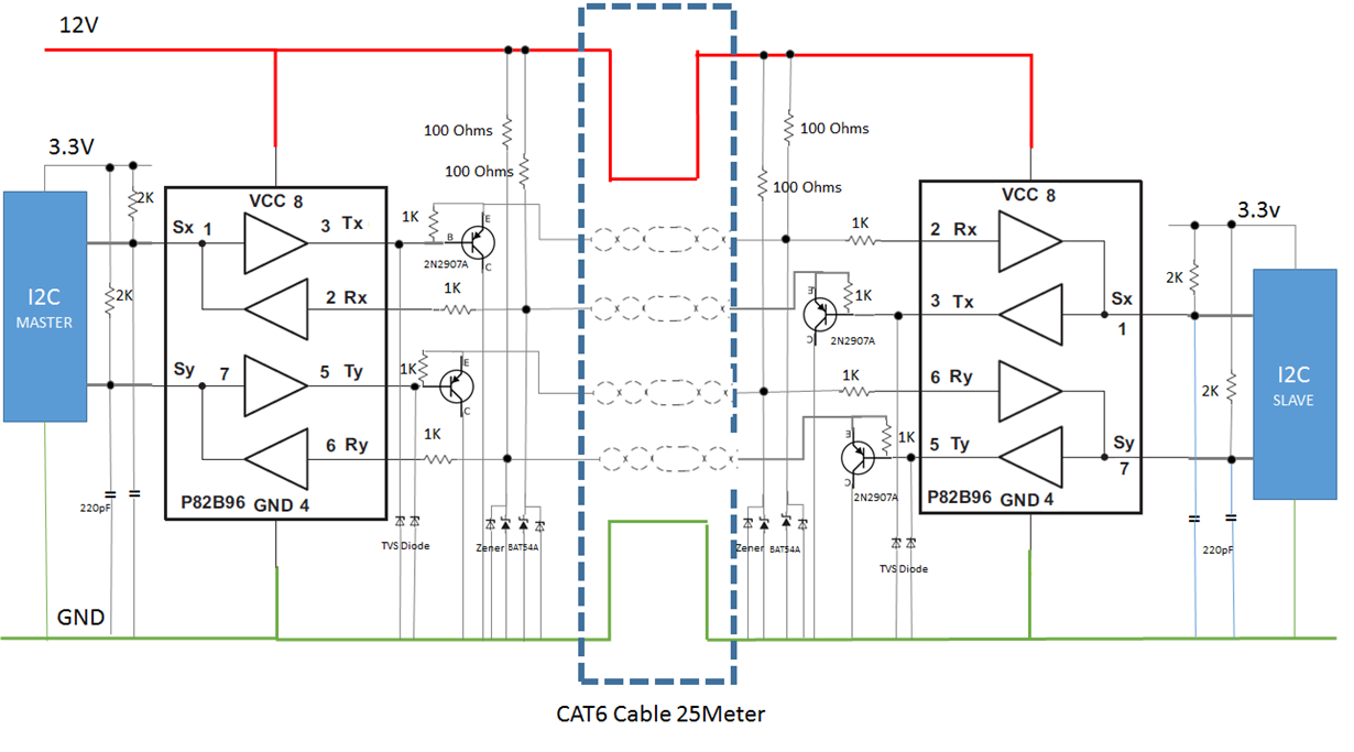
We are unable to establish I2C communication using P82B96 over 25 meter CAT6 cable. I have attached our detailed connection diagram. The lines are at 12V (sensing 10.86V only due to cable voltage drop). The MCU's on either sides are EFM32 series MCUs from Silicon Labs. The connections in diagram are similar to the ones suggested in P82B96 Data Sheet except the PNP Transistor. The PNP transistors here act as current sinks on lines, there by both enabling relatively higher current transmissions on CAT6 lines (faster transmission rates) and protecting P82B96 Tx pin from high current.

I2C communication between the MCUs is working fine with jumper wires (MCU's pins connected directly using 15cm wires) - so no program issue.

We tried various bus clock speeds - 400, 100, 30, 3 kHz, but no luck. We broke our oscilloscope and it will take a while before we can test the receive signals on scope. So, we tested the P82B96 pin voltages on either side of CAT6 cable by setting the MCU pins to high and the readings are below (readings are same for P82B96 on either sides of cable),

1) Sx and Sy pins are at constant 0.66V when the MCU pins are high(3.3V) and at 0V when MCU pins are low(0V)

2) Rx and Ry pins are at constant 0.3V when the MCU pins are high and at 0V when MCU pins are low

3) Tx and Ty pins are at 9.85V

4) P82B96 Vcc pin is at 10.86V

5) Voltage Across Transistor Emitter-Collector 9.86V

The voltages on Sx and Sy pins are at constant 0.66V even though they are pulled-high to 3.3V using 2kOhms pull-ups and MCU pins are driving high (3.3V). According to P82B96 datasheet, "The VOL level of 0.8V is needed to avoid locking/latching both sides of the P82B96 in a low state". Is the voltage locked at 0.66V because of this.

But at a 3.3V power supply, the EFM32 MCUs Input logic levels are  0.99V Max for Logic Low and 2.31V Min for Logic High. So, we suspect the logic high of P82B96 Sx pin is read as Logic Low by MCU. Does this explain why the connection is failing? 

Also, even though the Rx and Ry pins are pulled high to 12V using 100 Ohms resistors, the voltage levels on pins is 0.3V. Is this expected? For the 100 Ohms pull-up resistor on these pins, the voltage on line side pin is 9.86V and voltage on Rx side pin 0.3V. So, is P82B96 internally pulling the voltage on these lines low? We checked the diode connections and they are well reverse biased and not shorted.

Could anyone please verify the voltages and let us know if they are as expected? Also, kindly suggest what could be wrong in our connection. We can run more tests and share details if required. Any help is highly appreciated.

Thanks,

Ravi

  • 25 m is quite a lot. Is the capacitance still below 4000 pF?

    This connection diagram looks not at all similar to figure 10 or 13 in the datasheet.

    Why do you think you need more than 30 mA? Does the actual circuit from the datasheet, without any changes, work?

    What are the voltage drops over the pull-up resistors in both states?

  • Hi ,

    To overcome the 4000pF capacitance limitation and faster voltage transmission, we are pushing higher currents on transmission lines using 100 ohms pull-ups and sinking that current at Tx pins using PNP Transistors. Hope this also explains why we are looking at currents higher than 30mA.

    Yes, although the circuit skeleton is derived from P82B96 Datasheet, we made few modifications to just suit longer cables.

    We did not test the circuit in datasheet. We can test and share the results if you feel that helps to solve our problem.

    The voltage drops over the 2K pull-ups on Sx and Sy are

    1) Logic 1 - Voltage drop 2.3V
    2) Logic 0 - Voltage drop 3.29V

    Hope these answer at-least few of your questions.

    Could you please let us know what should be the working voltages on Sx and Sy pins for both states. As posted earlier we are sensing only 0.66V for logic high Sx pin, which unfortunately falls below the minimum threshold for MCU logic high.

    Regards,
    Ravi
  • Sorry, I meant the 100 Ohm pullups.
    (The Sx/Sy circuits look OK, the problem must be with the cable's circuit.)
  • Hi Clemens Ladisch (508254) ,

    First of all, let me thank you for taking time to review our connections.

    For MCU logic 1, Voltage drop across 100 Ohms is 0.94V and for logic 0, its 5.66V. The voltages across various circuit components for both logic states are below.

    One quick observation, for both logic states the voltage across Rx & Ry pins is almost similar. Is this expected? If that's so, may be I do not need Zeners/Schottky on Rx & Ry pins any longer. Or, you think the Zener/Schottky on the Rx & Ry pins are shorting the respective pins to ground?

    Vcc: P82B96 Supply pin voltage

    Vec: Transistor Emitter-Collector voltage

    Veb: Transistor Emitter-Base Voltage

    Column Headers in Orange are components on High side (12V) and Headers in Green are components on Low side (3.3V). 

    Do you spot anything wrong now? Please let me know if you need further information.

    Thanks,

    Ravi


    Vcc 100 1K BAT54A TVS D Tx Ty Rx Ry Vec Veb 2K 2K Sx Sy
    Logic 1 10.7 0.94 9.48 0.29 9.79 9.79 9.79 0.29 0.29 9.8 0 1.18 1.18 2.05 2.05
    Logic 0 6.7 5.66 0.76 0.2 0.08 0.08 0.08 0.2 0.2 0.8 0.73 3.29 3.29 0.02 0.02
  • Apparently, the logic 0 state horribly overloads the power supply.

    In the logic 1 state, there should be no voltage drop (and no current) over the pull-up resistors. 0.94 V corresponds to a current of 95 mA, all of which flows into the Tx/Ty outputs. This is above the recommended operation conditions.

    Which 1K resistors did you measure? The Rx/Ry resistors should have no current in any state, and the base-emitter resistors should never be able to go above 0.7 V. Strange.


    I suspect the problem is related with the PNPs in common-collector configuration. I'd have tried NPNs (or N-channel MOSFETs) with an inverting logic gate to drive the base/gate.

  • Hi ,

    We removed the Transistors and the circuit is just working fine. Thanks a lot.

    We are still unable to establish a communication link through P82B96 and request your kind help. Am sharing the logic analyzer screen shots.

    Below is the waveform at the Master pins when Master and Slave I2C pins are directly connected with 15cm wires without P82B96.

    The below picture shows the wave-forms at Master when Master and Slave are connected over 25m CAT6 cable through P82B96

    And the wave-forms at the Slave end are below,

    A closer look at the Master and Slave wave-forms reveal that although the Master Signals are received perfectly at the Slave end, the ACK sent by the Slave after the Address Match is not received at the Master (Slave is pulling the SDA line low but still the SDA line at Master is high). This is causing the Master to abort the transmission with a STOP bit.

     Any suggestions to make this work please.

    Thanks,

    Ravi