This thread has been locked.

If you have a related question, please click the "Ask a related question" button in the top right corner. The newly created question will be automatically linked to this question.

TXB0104 doesn't drive to GND

Other Parts Discussed in Thread: TXB0104, TXS0104E

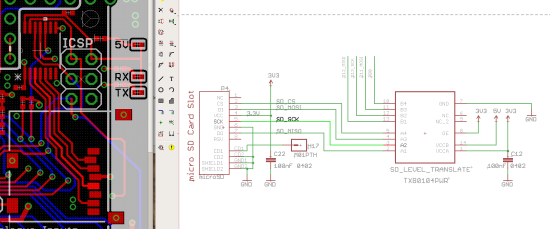
Using a TXB0104 in a simple 5V/3.3V translation application. An AVR ATmega on 5V side, and a uSD Card cage on the 3.3V side. There are no additional pull-up or pull-down resistors on the 3.3V side.

The below image shows the schematic and the board layout.

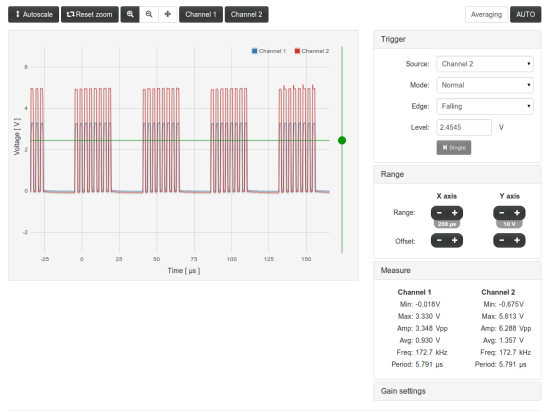
With no uSD card inserted the SCK signals are correctly translated, as per the below example.

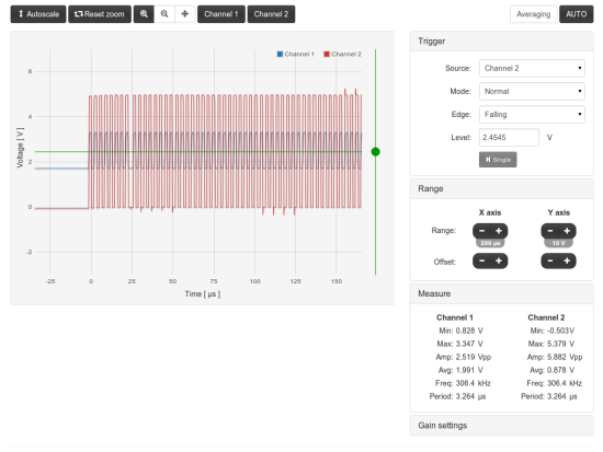
With the (any) uSD card inserted the SCK output signals on the 3.3V side never drive to 0V, instead they remain above 1V.

This is the problem.

What is missing from this layout to prevent this obvious voltage translation application working as intended?

  • Hi,

    Thanks for using the part, based on your test result, it seems there is a integrated pull up resistor inside uSD card for the SCK signal. as you know there  is a 4Kohm serial resister inside the TXB0104, if uSD card SCK signal has the 10Kom pull up resistor inside, it will cause the VOL raise to be aboout 1V.

    you  can check with uSD card vendor or the uSD card datasheet to confirm it, or do the test on the uSD card by yourself to check.

    If so, the suggesiton is you can replace  the TXB0104 to TXS0104, the p2p replacement may be possilbe, it based on the package itself.  


  • Thank you for your suggestion to convert the TXB0104 to a TXS0104E chip.

    I have done so by a pin compatible swap, and there has been an improvement in the situation.

    Below, a logic trace of a uSD card initialization.

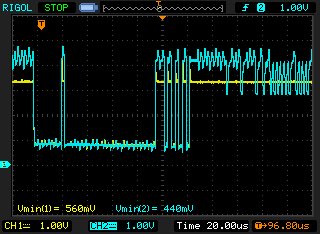
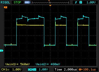
    Associated, the oscilloscope trace of MISO 3v3 yellow and MISO 5v blue, near the time when 0xAA is being transmitted.

    A higher resolution view of the same section, identified by the orange indicator triangle. Timing of signal transitions is very accurate.

    Issues.

    1. The VccB side 5v output signal is very variable and noisy. This is particularly so when other lines are being driven. See where 0x77 is being transmitted on MOSI, there is a voltage drop and significant ringing on MISO (shown on the oscilloscope). I have added 2u2F capacitors to 100nF bypass capacitors on both VccA and VccB to try to avoid this issue. The situation was slightly improved, but remains as shown. Is this normal? Can it be avoided?

    2. Most uSD cards fail to initialise. I have compared identical firmware initalisation routines on hardware using simple voltage divider circuitry for voltage translation, with the new TXS0104 solution. All uSD cards properly initialise and test using older simple circuitry design. Most (9 of 11) of these same cards fail to initialise when using the TXS version.

    The indicated symptom is that the cards fail to continue to respond to AMCD41 commands (with HCS bit) with 0x01 (when in idle state) and then fail to respond with 0x00 when ready to proceed. The MISO line just goes high 0xFF and does nothing more.

    This is perplexing. It is not a code issue. The code is identical. It doesn't seem to be a TXS0104 issue, but is it the only variable that has changed. Are there any thoughts about this?