This thread has been locked.

If you have a related question, please click the "Ask a related question" button in the top right corner. The newly created question will be automatically linked to this question.

TXB0104

Other Parts Discussed in Thread: TXB0104, TXS0104E
We have a issue when using we are interfacing TXB0104 and SN75451B.

SN75451B is used for TX driver for Fibre Optic Transmitter HFBR-1412PZ and operates at 5V, TXB0104 is used to convert UART 3.3V level to 5V level

Issue:
When We provide UART signals (5V) TTL level directly to SN75451B and to FO converter, it  works

But when we provide same UART signals (@ 5V) which are  level converted from 3.3V through TXB0104, FO is not working,

Schematics for TXB0104 and FO with SN75451B are attached.  

Sch.pdf

  • Hi Rekha

    Is there a receiver connected to the Rx signals?

    Have you confirmed that the level translation occurs as expected- ie, 5V at the output ports of the TXB0104? Take into consideration just the TXB device by isolating it to debug.

    Thanks

  • Hello Jennifer Joseph,

    Yes, full receive path is working fine. (from opto, to txb0104 and then processor)
    The working of the TXB0104 was independently tested. The o/p voltage levels @ TXB0104 are 5V.

    Regards,
    Rekha
  • Thank you.

    Can you please provide waveforms showing B2, B4 of U19 and 1Y, 2Y of U17?

    Also for this part, an external system driver must supply more than ±2 mA of current.


    Thanks

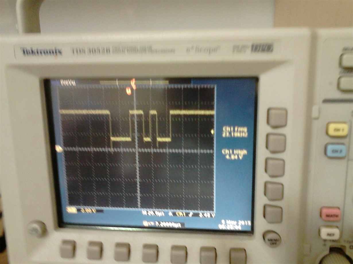
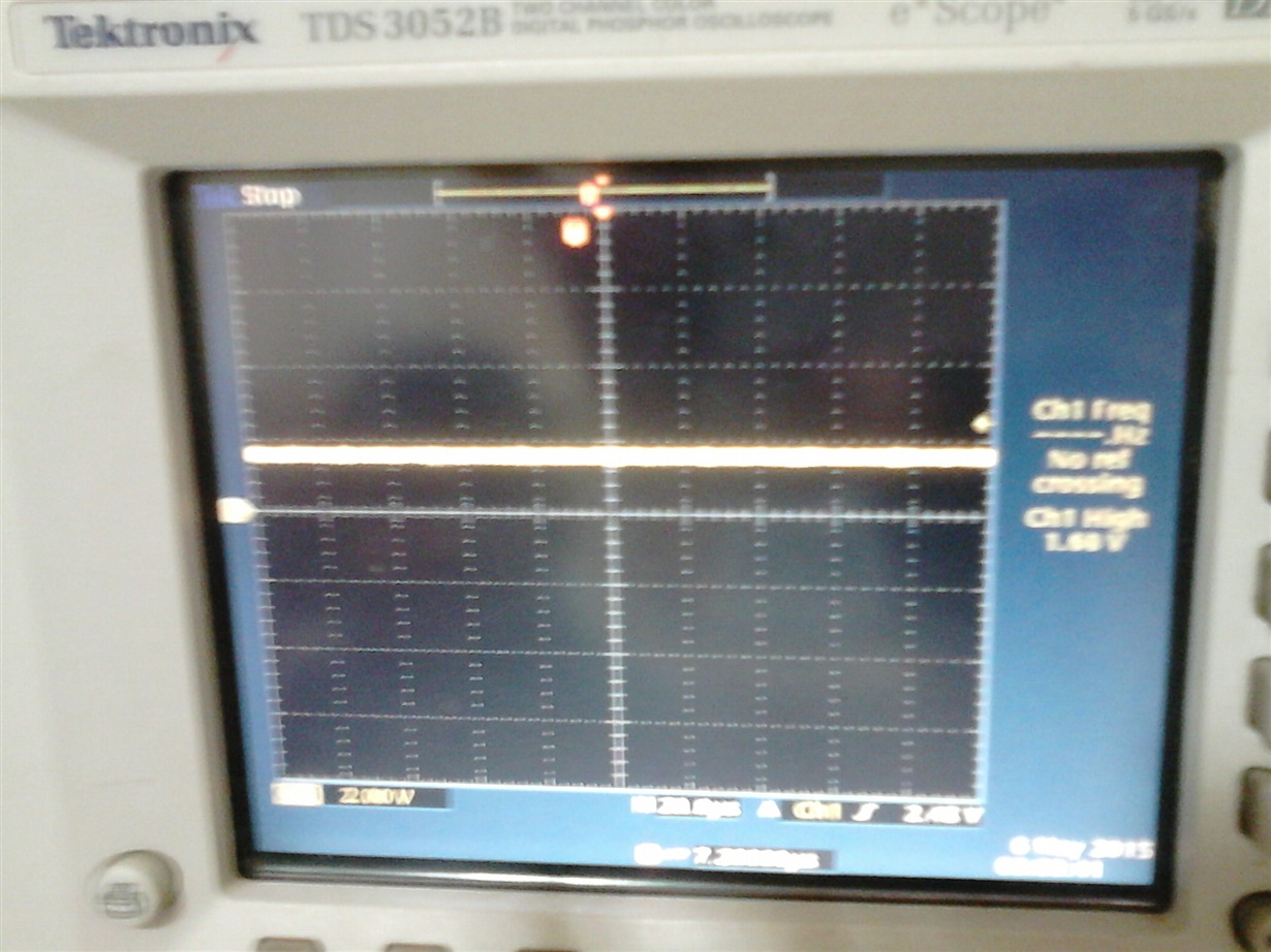
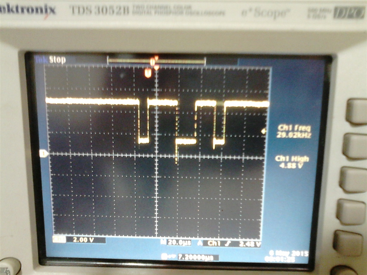
  • Attached are the snapshots of the signals at U19-B2, U19-B4 & U17-1Y.  I could not take for U17-2Y as it was always showing 0.  We are investigating the issue.

    Pl. elaborate on external system driver requirement.

  • Hi Rekha

    Thanks. What is contributing that 1.2V offset in the first waveform?

    TXB-type translator have a 4K series impedance buffer. This part is strong enough to hold the output port high or low during a dc state, but weak in that the 4-kΩ impedance buffer can be easily over-driven by a system driver connected to the A or B port when a bus direction change is desired.

    An external system driver must supply more than ±2 mA of current to reliably overdrive the hold provided by the weak buffer.

    Good application note on the TXB translators:

    http://www.ti.com/lit/an/scea043/scea043.pdf

    Thanks.

  • Dear John Joseph,

    Following are observations from our side,


    1) At SN751451B input 1B,2B  there is dc level of 2V always,

    2) when we drive external TTL signal of 5V  directly to 1B, levels at 1B is at 5V and Fibre optic is working fine,

    snapshot at 1B with external 5V TTL applied is attached,

    levels are 5V

    3) when level converted signal from TXB0104 is applied at 1B of U17, there is dc shift of 1.2V, as attached in the previous post,
    due to which FO is not working,

    when Direct 5V signal is applied, levels are fine as shown, when level shifted 5V is applied, dc shift of 1.2V is present.

    let us know, how do we resolve this issue,

    Regards,

    Vijay

  •  


    Hi Vijay

    Thank you for confirming on the 1.2V offset. I wanted to make sure it was real and not just a bad grounding effect.


    1)      Please help to answer questions a) to e)

    a)      There is a 4k series resistor on input and output signal. Please check the equivalent resistor of probe and signal source if there is no any external resistors on PCB board.

    b)      Measure the resistance between OE and GND when power is zero.

    c)       Does the 1.2V offset change with connecting and disconnecting a probe?

    d)      Confirm if the micro/processor output current is more than 2mA (it most likely is, just a confirmation for debug)

    e)      Power up sequence of the supplies


    2)      Please check on below, I suspect this might be the likely cause for the dc offset:

    Make sure the input pin is not floating when you measure the input or output signal. The TXB0104 needs to be at a determined state at input. For floating inputs, the output signal state is not well defined.

    *note is page 5 of the datasheet ((1) The A and B sides of an unused data I/O pair must be held in the same state, i.e., both at VCCI or both at GND.)


    Thanks

  • a) There is a 4k series resistor on input and output signal. Please check the equivalent resistor of probe
    and signal source if there is no any external resistors on PCB board.
     
    ans: there is no external resistor on pcb board, we couldn't measure the same
     
    b) Measure the resistance between OE and GND when power is zero.
     
    ans: in range of Mega Ohm
     
    c) Does the 1.2V offset change with connecting and disconnecting a probe?
     
    ans: 1.2V offset doesnt change with connecting or disconnecting probe
     
    d) Confirm if the micro/processor output current is more than 2mA (it most likely is, just a confirmation
    for debug)
     
    ans:  o/p current is greater than 2mA, we are using CP2108 chip for UART, we tried driving the TTL from different chips also, o/p current is greater than 2mA 
     
    e) Power up sequence of the supplies
     
    ans: Both VCCA and VCCB are powered at the same time.
     
    2) Please check on below, I suspect this might be the likely cause for the dc offset:
    Make sure the input pin is not floating when you measure the input or output signal. The TXB0104 needs
    to be at a determined state at input. For floating inputs, the output signal state is not well defined.
    *note is page 5 of the datasheet ((1) The A and B sides of an unused data I/O pair must be held in the
    same state, i.e., both at VCCI or both at GND.)
     
     
    ans: Input is not floating, TTL signal is connected always during the testing, it is at 3.3V(VCCA) level
     
     
    It is to be noted that, TXB0104 is working independetly, waveforms at o/p of TXB with and without driver is attached.

    with driver was attached in the previous post,

    without driver is attached below, its levels are OK,
     
     
    Thanks
    vijay

  • Hi Vijay

    Thank you for all the information. Lets focus just on the TXB0104 inputs then.

    1)It will be nice to see waveforms of Vcca, Vccb, OE, one input port and respective output port. If it is too cumbersome to send waveforms, you can verify it yourself.

    My thought process behind asking for the waveforms above is to look at the input transition rise/fall rate. As mentioned on page 6  in the datasheet it must be 30ns/V max.

    Also, to check on anything amiss on the inputs coming in to the TXB0104.

    2) I know that you have looked at this, but please make sure that at any point in time, none of the unused I/O are floating.

    3) One final aspect will be to look at the layout. When you tested with/without driver, I assume these were 2 different boards?

    Thanks

    Jennifer


  • Dear Jennifer,

    The issue is resolved,

    We replaced the TXB0104 part with TXS0104E part,

    with TXS0104E waveforms are fine with no dc shift, and fibre optic is also working,

    Thanks for all the support you guys provided,

    Regards,

    Vijay

  • Glad to hear Vijay! Please close this thread if possible. Thanks.