This thread has been locked.

If you have a related question, please click the "Ask a related question" button in the top right corner. The newly created question will be automatically linked to this question.

TPS65987D: Workflow or example code to use as PD3.0 source

Part Number: TPS65987D
Other Parts Discussed in Thread: TPS65987, , TPD6S300A

Currently we are wondering if there is an example code, config file or a description of a workflow to use the TPS65987 as a power source for a mobile device. We are checking different combinations of the poorly described registers but even after a few hours we see no success. 

We would be glad about any hint to configure the IC as a power source to provide our MCU all information to configure the external power source.

  • Hello,

    Our TPS6598x Application Customization Tool has example templates that would fit your application. You can download the tool from here:

    If this answers your question, PLEASE select This resolved my issue

    Thank you,
    Eric

  • Hi Eric,

    thank you for your quick response. We don't have the FTDI device and I'm wondering if the templates can be used without the tool?

    We have our own MCU and a I2C link to the TPS65987. In best case we can have a list of register values we have to set.

    Thank you very much.

  • Hello,

    That's correct, it would give you a list of register settings at the very least. Additionally, it could be used to generate your low region binary that you can push to the TPS65987D over I2C during bootup. This app note explains that process in greater detail:

    If this answers your question, PLEASE select This resolved my issue

    Thank you,
    Eric

  • Hello,

    unfortunately we did not yet have success in neogtiating a PD contract.

    I think one of the main problems is, that the TPS65987 is always reporting that it is acting as a legacy source (register 0x1A, bits 25:24, 10b: PD Controller is acting like a legacy source. It will not respond to USB PD message traffic.)

    Why is the chip entering this legacy mode? I could not find a description for this behaviour.

    Thank you,
    Christian
  • Hi Christian,

    I would suggest checking your ADCIN1 pin voltage during boot. It sounds like you may be entering one of the default configs and not changing the register settings to your desired behavior. You can check the boot mode pin strapping in Table 5 of the datasheet.

    If this answers your question, PLEASE select This resolved my issue

    Thank you,
    Eric

  • Hi Eric,

    I checked the voltage and it is 0V as expected. Our PCB has a pulldown on the pin, as well as SPI MISO. This would mean Configuration 1 is loaded per default, which is also what I see in the Tx Source Capabilities register (0x32). How does this setting affect the "legacy source" problem?

    During my startup routine I set the TX Source Capabilities Register to have 3 PDOs, setting the Power Path selection to PP2 (again because of our PCB) etc. I also set Port control register (0x29), Golbal System Configuration (0x27) and PD3 Config register (0x42). Is there anything else I have to check?

    Thank you,
    Christian
  • Hi Christian,

    Are you pushing a patch to the device? It seems like you are booting into a default config and then changing the register settings. Are you confirming that the register settings are changed by reading the registers back?
    I would suggest following the steps in this app note for programming a spi-less system over I2C: www.ti.com/.../slva972.pdf

    Thank you,
    Eric
  • Hi Eric,

    thank you again for your support. Maybe I have to explain our configuration a little bit more.

    We have a microcontroller that is communicating with the TPS65987 using I2C2. ADCIN1 and ADCIN2 are directly connected to GND. After system reset, our microcontroller tries to configure the TPS65987 as a power source.

    Out intention is to use the TPS65987 to negotiate the PD contract and provide our microcontroller the information how to program the output of an additional, controllable DCDC converter. The TPS65987 should additionally switch the output of this DCDC converter.

    Till today, we didn’t come to the point, that the TPS65987 provide us the necessary information. It switches the output on (depending on configuration), powers the sink with 5V but didn’t negotiate PD handling.

    Christian noticed today, that the legacy source register is active and the datasheet said that in this mode, the IC does not respond to PD traffic. Now we are wondering if this may a hint to the issue.

    We will check the application note tomorrow, maybe it helps.
  • Hi DH,

    Please let me know if additional assistance is needed after reviewing the app note.

    Thank you,
    Eric
  • Hi Eric,

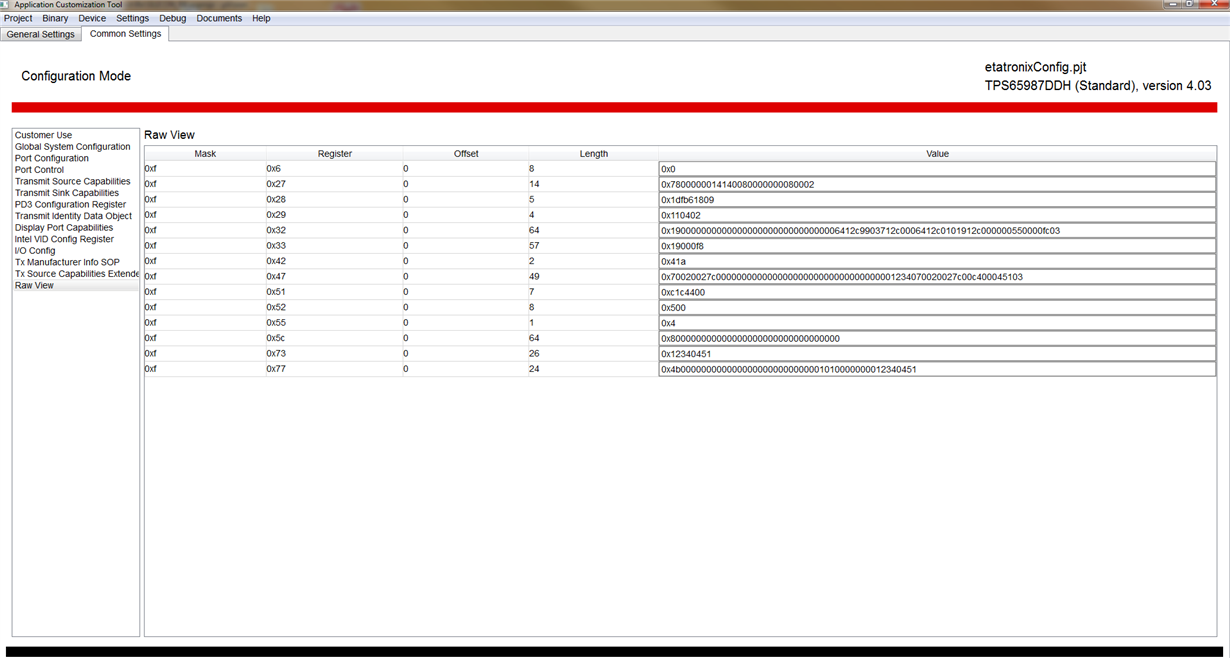
    unfortunately we still did not have success. I configured our use-case with the application customization tool and configured the registers according to the given values.

    Config TPS65987

    The system is now behaving like this: periodically switching the output for 300ms, at the end of the power-on phase the CC line is going low. Do you have any hints what may be wrong? Are the register values correct? I read the register values back to make sure they are configured properly.

    Edit: One thing I noticed is, that the config tool is setting saying register 0x51 has 7 bytes, whereas the host interface document states the register is only 6 bytes long.

  • Hi Christian,

    I would suggest connecting your system to our debug tool over I2C using either an FTDI or Aardvark adapter. This would allow you to enter debug mode with our GUI tool and very accurately read back what configuration is active on your board. It is difficult to determine which state the device is actually in without this type of debug.

    Thank you,
    Eric
  • Hi Eric,

    I did as you suggested. But still no luck.

    tps65987_snap.zip

    I exported the attached snap. Could you please have a look at it?

    Thanks,

    Christian

  • Hi Christian,

    I see that you have 5V, 9V, 15V, and 20V set in your source capabilities. however, I do not see any GPIOs used to control the voltage of an external regulator. How are you adjusting your source voltage to ensure 20V is able to be sourced? You could always just have the 5V Source PDO only to avoid this issue.

    If this answers your question, PLEASE select This resolved my issue

    Thank you,
    Eric

  • Hi Eric,

    Christian is out of office today and we are in a hurry so I hope it's ok that I try to assist.

    Our board contains an controllable DC/DC converter connected to PP_HV2. The intended job of the TPS65987D is to handle the power delivery communication with the application. What we try is that the TPS65987D negotiates the PD contract, provides us all information of the application and we adapt the output voltage of the mentioned DC/DC converter to the results the TPS65987 negotiates.

    Our understanding (or maybe misunderstanding) is that our DC/DC converter starts with 5V and the TPS65987 connects this voltage to the application (or load). With this voltage, the negotiation starts. After a while, the TPS65987 knows what's the requested voltage and current of the load and we can read this information using I2C. With this information, we program our DC/DC converter to the desired voltage. Can you please confirm that this will generally be possible.

    Thank you Eric.
  • Thanks, DH.

    In theory that is possible. However, it would be a challenge with the timing. If the voltage does not ramp quickly enough, the PD controller would do a Hard Reset which I believe is what you are seeing.

    I would suggest using the GPIOs to control the DC/DC converter like on the TPS65987EVM as this would remove the timing complexities.

    If this answers your question, PLEASE select This resolved my issue

    Thank you,
    Eric

  • Hi Eric,

    Thank you for you quick response. Unfortunately this isn't possible with the current design, but I'm not sure if we really see a hard reset. Can we measure this reset at the reset pin, because we don't see any level changes there?

    Where can we find further information related to the timing of the TPS65987? The settle time (tSrcSettle) specified in the USB PD-Spec looks ok for our DC/DC converter.

    I can't find any information in the datasheet that we have to use GPIOs to control the input voltage of the device. Do you have further information.

    Thank you.
  • Hi DH,

    Do you have a PD analyzer available?
    This could be used to see which voltage is negotiated and if a Hard Reset is occurring.

    Thank you,
    Eric
  • No, unfortunately not. Do you have a recommendation for an analyzer?
  • The Total Phase PD analyzer is a good option:
    www.totalphase.com/.../
  • Thank you very much.

    Are you sure that there is no option to use our circuit as mentioned earlier. This will make it ways easier because the PCBs are still produced.
  • Hi DH,

    If you could get the DC/DC to output the correct voltage at the correct time with this scheme then it is usable. However, it is very difficult to debug without having a PD analyzer to see what is going on.

    Thank you,
    Eric
  • Hi Eric,

    I don't think a PD analyzer will help us much, as I believe the problem to be much more basic. When monitoring the CC line with an oscilloscope I don't see any communication. CC line  is just static. I believe communication should have a baud rate of 300kbps.

    Also I don't think we are experiencing a hard reset, as all the data is still what we configured (that is Tx Source Capabilities, Port config, etc).

    In the State Machine Trace it always is like this:

    Port 0 PD 0x2f = PEState_Enable_VBUS

    Port 0 PD 0xbe = PEState_Disabled

    Right after enabling VBUS the state machine is disabled. Why is that?

    A few years ago I was working with BQ battery chips, they had an extended manual for implementers. Is there something similar available for the TPS?

    Thank you,

    Christian

  • Hi Christian,

    Please keep in mind that there are two CC lines on the TPS65987D to handle the cable flip. Are you seeing the same behavior on both? There would be no PD communication if you are just connecting a Type-C only device. You will only see PD messaging if you connect a PD compliant device. If you are seeing the 5V VBUS get enabled and disabled, there is most likely a Reset event. I would ensure your schematic is closely matching the TPS65987EVM. The EVM user's guide for the TPS65987EVM or TPS65988EVM could be used as an implementation guide.

    Thank you,
    Eric
  • Hi Eric,

    yes I know, I checked both CC lines.

    In our PCB the VBUS1 output is shorted to ground, as we don't use it. Which is right according to the datasheet.

    But when the TPS is acting as legacy source it says VBUS is at vSafe0V (less than 0.8V), even though I can measure 5V at the output. So I am wondering if VBUS1 and VBUS2 have to be connected to the same node at the output. If not can you explain why VBusStatus is at 0?
  • Hi Christian,

    Do you have a way to connect both VBUS1 and VBUS2 to the VBUS node of the Type-C connector on your PCB?

    Thank you,
    Eric
  • Hi Eric,

    connecting both nets isn't easy because the boards are manufactured and the components placed. If this will be the solution, we can try it, but it's not easy to test. Do you think it's worth testing?

    Are you in contact with the design group of the IC and can ask if this will solve our issue? If not, do you think it's possible to bring us in direct contact with them? For me it looks like our issue is a very fundamental one. The IC is pretty new and maybe our configuration is not the same than yours.

    Regards,

  • Hi DH,

    This would very likely resolve your issue. I am working internally to get the datasheet updated as it appears the pin descriptions for VBUS1 and VBUS2 have an error in them. VBUS1 and VBUS2 pins should be tied together on the TPS65987D and both should go to the Type-C connector. I apologize for the confusion.

    Please test your board with VBUS1 and VBUS2 both tied to the Type-C Connector VBUS.

    If this answers your question, PLEASE select This resolved my issue

    Thank you,
    Eric

  • Hi Eric,

    Thank you for your support. Yes, looks like this solves the issue...

    Our circuit looks like specified in the datasheet and I'm pretty sure, that there are other companies with the same issue.

    I'm wondering if there is a firmware available from TI that works as an interims solution. The boards are manufactured and it would be needless to throw several thousands of Euros away.

    Regards
  • Hi Eric,

    as Dominik already said, connecting VBUS1 and VBUS2 together to the same node did the trick. We can negotiate a power contract and charge a tablet at 20V. However this only works after the first connect. If I unplug the connector and plug it back in it won't work. Any suggestions where the failure might be?

  • Hi Christian,

    That's an odd failure. Are you changing any of the register values between connections? If nothing is changed in the configuration, there maybe something in hardware changing between connections.

    Thank you,
    Eric
  • Hi Eric,

    register values are unchanged.

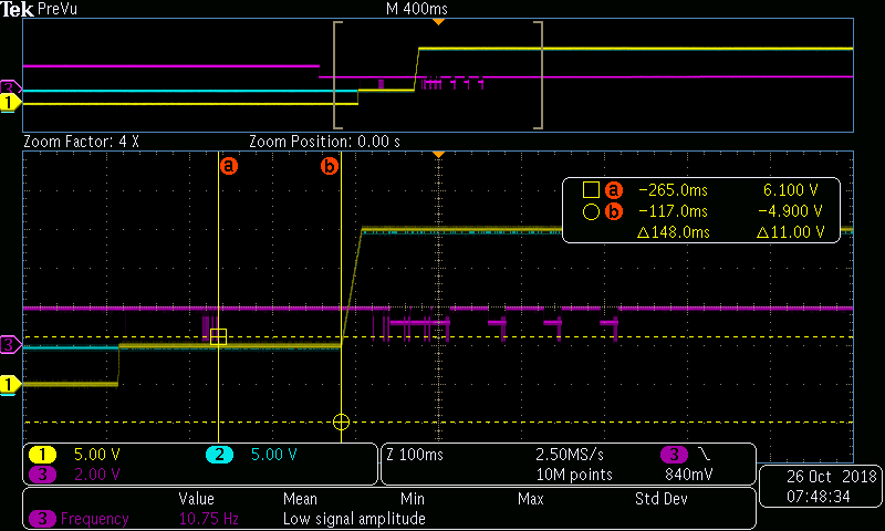
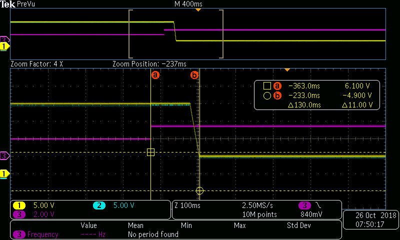
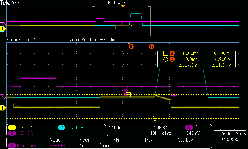
    I looked a little deeper and found that the TPS is negotiating the power contract again correctly, our DC/DC is setting the voltage to 20V. But the TPS is beginning to limit the voltage at 6.1V and VBUS is subsequently dropping to 0V. For a short time I saw the in the hardreset details the following bit set "Required by policy engine, UnableToSource.".

    Thank you,
    Christian
  • Hi Christian,

    We would send the "UnableToSource" Hard Reset if the VBUS voltage does not ramp to the correct level quickly enough. Is the voltage output from your DC/DC reaching 20V in the correct time?

    Thank you,
    Eric
  • Hi Eric,

    I attached some screenshots from the oscilloscope. To me it looks like the voltage is rising fast enough. 

    Yellow: VBUS

    Blue: VDC

    Red: CC line

    1st connect

    1st disconnect

    2nd connect:

    I am not sure why the CC line is going to 3,3V shortly before the negotiation.

    I also noticed, that the TypeCStateRegister (0x69) is reporting the Unattached.SRC state after disconnect, but the TPS is still sourcing VBUS, which is not right according to USB Type-C Specification Chapter 4.5.2.2.7.1 Unattached.SRC Requirements

  • Hi Christian,

    Is it possible for you to obtain a TPS65987EVM? I could not reproduce the behavior you are seeing on my side and it is very difficult to debug without further information.

    Thank you,
    Eric
  • Hi Eric,

    Christian is on vacation but we don't have the TPS65987EVM here. Maybe you could send us a system?

    Regards,

    DH
  • Hi DH,

    Unfortunately, we cannot send a system. These are orderable from the TI e-store.

    Thank you,
    Eric
  • Hi Eric,

    our problem is still open and and to be honest, I'm not sure how the EVM should solve our problem. Even if we can confirm, that the behavior of the EVM is not the same as you said, this will not solve our issue. Is there an FAE on your side we can have a conference call with?

    We use the system as specified in the datasheet and for me it looks like if he don't find a solution soon, we have to choose another IC to minimize our design risk.

    Regards,

    DH
  • Hi DH,

    The behavior of the device does not change from one connection to the next unless there is a change in the configuration or the hardware. I am unable to reproduce this failure locally and suspect it may be something with your hardware that prevents the second connection. Having an EVM would help you narrow down what is going on.

    Thank you,
    Eric
  • Hi Eric,

    thanks for your response. For my understanding, the complete behavior of your IC gets controlled with the corresponding registers and it would also be an option that an expert of the IC checks our registers in detail. The external configuration of the IC is straight forward and our DC/DC converter works as specified in the USB specification. More than that, it's working every first time, but after disconnect and connect of USB, the handling fails. I'm pretty sure this have nothing to do with our hardware.

    Maybe you understand, that it's very unsatisfying buying more and more hardware to notice, that there is still a problem with the IC or the datasheet, not our hard- and firmware...
  • Hi Eric,

    could you please explain what is expected at PPHV1 if we don't use PP1. VBUS1 and VBUS2 have to be connected to the same node. But what about PPHV1 and PPHV2? Can they be independet? At the moment PPHV1 is connected to VBUS (routing of our PCBmakes it hard to disconnect PPHV1 and VBUS1). Is this ok or a possible fault?

  • Hi Christian,

    Yes, this would explain the failure you are seeing. This would be equivalent to one of the power paths being shorted. Please connect VBUS 1 to VBUS 2 only. PPHV1 and PPHV2 can be independent.

    Thank you,
    Eric
  • Hi Eric,

    I know. But since we only use PP2 to switch VBUS, PPHV1 is only seeing VBUS when PP2 is conducting (as you can see from the screenshots a few post before, VBUS is 0 at fist connect). Therefore, when PP2 should be closing PPHV1 should no longer be seeing VBUS.

    We tried it anyway, with little result. The same failure is still persistent.
  • Could you please check the SCM file in the attachment if there is anything wrong? Please keep in mind, that VBUS1 and VBUS2 are already connected to the VBUS node and PPHV1 is connected to PPHV2. Thank you!

    SCM_USB_Type-C.pdf

  • Hi Christian,

    If you have VBUS1 connected to VBUS2 (and not grounded). PPHV1 may remain grounded or connected to PPHV2. You could also try removing D901 as this may cause some interference on the CC lines. If ESD protections is required on the CC lines, I would recommend looking at the TPD6S300A.

    Thank you,
    Eric
  • Thank you, we will check if there is an issue with the ESD Diode.

    You don't see an issue with the schematic, do you? Why do we than see the behavior Christian explained earlier. Do you have another idea? Is there a standard configuration you can provide using the IC as we do, with an external DCDC converter and no flash memory?

    Regards,

    DH

  • Hi DH,

    If VBUS and PPHV (both 1 and 2) are correctly connected, I don't see any issue outside of potentially the ESD diode (D901).
    The defaults configurations on the 987 only output 5V, there is no default configuration to output 20V in the manner that you are. This adjustment would all need to be made through your EC.

    Thank you,
    Eric
  • Hi Eric,

    we tried to make it work without the diode. But still no luck. I think we need some further in-depth assistance.

    Thank you,

    Christian

  • Hi,

    I am attaching 4 snaps of the system to investigate further on the problem. One is before connecting anything, then 1st connect, 1st disconnect and 2nd connect. We would appreciate it if you could shed some light on the problem based on the snaps.

    Thanks,

    Christian

    snap_After1stDisconnect.zip

    snap_After1stConnect.zip

    snap_After2ndConnect.zip

    snap_BeforeConnect.zip

  • Hi Christian,

    Thank you for the logs, there is one more thing that you can try that would improve the behavior. It seems that you are running completely out of the devices ROM and changing the config during run-time. I would suggest that you change the ADCIN1 behavior to accept a patch from the EC, the following app note explains how this is done:

    We have made many improvements to the TPS65987D through the patch and changing to this method would ensure all these improvements are present on your system.

    If this answers your question, PLEASE select This resolved my issue

    Thank you,
    Eric

  • Hi Eric,

    okay we will try. But where do I find the patch file for the TPS?

    Regards,

    Christian