This thread has been locked.

If you have a related question, please click the "Ask a related question" button in the top right corner. The newly created question will be automatically linked to this question.

DS90UB914A-Q1: I need GPIO2 & 3 to be input, but the datasheet is confusing

Part Number: DS90UB914A-Q1

Looking at the SNLS499B –APRIL 2016–REVISED OCTOBER 2016 datasheet, table 7, register 0x1E, page 40:

7 GPIO3 Output Value RW 0 Local GPIO Output Value This value is the output on the GPIO pin when the GPIO function is enabled, the local GPIO direction is Output.
6 RSVD Reserved.
5 GPIO3 Direction RW 1 Local GPIO Direction. 1: Input. 0: Output.
4 GPIO3 Enable RW 1 GPIO Function Enable. 1: Enable GPIO operation. 0: Enable normal operation.
3 GPIO2 Output Value RW 0 Local GPIO Output Value This value is output on the GPIO pin when the GPIO function is enabled, the local GPIO direction is Output.
2 RSVD Reserved.
1 GPIO2 Direction RW 1 Local GPIO Direction. 1: Input. 0: Output.
0 GPIO2 Enable RW 1 GPIO Function Enable. 1: Enable GPIO operation. 0: Enable normal operation.

Since GPIO2 and GPIO3 look identical, I will just use GPIO3 as my example.

Register bit 7 ONLY STATES THE OUTPUT CASE.

This is confusing. What I expect is, if bit 4 = 1 for active; bit 5 == 1, GPIO3 is an input AND the bit 7 will reflect the current state of GPIO3 external pin #25.

It is confusing because the description only talks about bits 3 and 7 as OUTPUT cases, NOT INPUT cases (GPIO2 should have bit 0 = 1 for active; bit 1 == 1 for input direction && bit )

Is that true? If the GPIO pin is active and input, what is specified as the output pin for the output case, is the input bit for the input case (which is the normal way these things usually work)????

(Register 0x1D for GPIO0/1 same verbiage...)

Thanks! ... bandit

  • Hi,
    The datasheet description is correct. The Output Value bit is for GPIO output only.

    There's no Value register bit for GPIO inputs.


    Best Regards,
    Charley Cai
  • Please forgive my confusion.

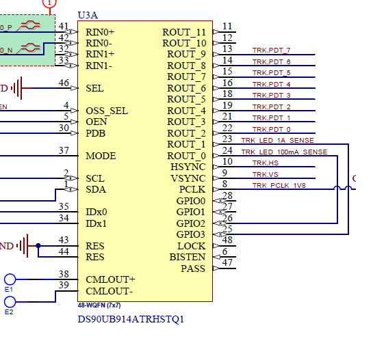
    This is what we want to do. We have an architecture which is very close to the '914 datasheet (SNLS499B –APRIL 2016–REVISED OCTOBER 2016) figure 17, page 24. We have the SERDES in 10-bit mode. However, we only need 8 bits for the image, so we have connected the "other 2" to a monitor circuit on the SER (a '913) side. Note since they will stay fixed to a values (high or low) during the entire frame, it should not matter the signals normally "wiggle" as a result of a normal frame. On the DES ('914) side, we pull the 2 extra off (ROUT_0/1)

    But now we need to read them. We see pins named "GPIO"  - General Purpose Input Output. The assumption is; if we "loop" from the image stream outputs to two of the GPIO pins (GPIO[2:3]), we can use I2C to read the corresponding registers to determine the values without needing to add more components.

    Looking at ('914) Figure 17 (page 23), it shows bi-directional flow for all FOUR (!!) GPIO[3:0] on the DES to the microcontroller. (so does the same figure 17 for the '913)

    Section 8.4.2 DS90UB913A/914A Operation with Pixel Clock from Imager as Reference Clock:

    • There are 4 GPIOs available in this mode (PCLK from imager mode)

    So - I am very confused. Breadcrumbs in the datasheet imply that any inputs into the DES would show up on the SER, but that does not make a lot of sense.

    If I configure a GPIO[3:0] pin as input, and set the pin to a valid signal, how/where do I read that input?

    If I am reading the '913 (SNLS443D –MAY 2013–REVISED OCTOBER 2016) datasheet, 8.3.5 General Purpose I/O (GPIO) Descriptions: 

    • The GPOs on the Serializer can be configured as outputs for the input signals that are fed into the Deserializer GPIOs

    • The DS90UB913A Serializer GPOs cannot be configured as inputs for remote communication with Deserializer

    The datasheets seem to be consistent between them (says the same thing) but inconsistent internally.

    Please advise.

    tanks ... bandit

  • Hi,

    When 914 GPIO is configured as input, valid signal present, and 913 GPO is configured to output, the signal will show up at 913 GPO pin. This signal then could be fed to microcontroller or other device to be read.

    For this device, the option to read GPIO data through register is not available.


    DS90UB934 supports the implementation you are trying to do, and can serve as a replacement for 914. The description is under 7.4.6.2 in DS90UB934 datasheet.


    Best Regards,

    Charley Cai

  • Not the solution I was hoping for.
    And - I am not the one who gets to decide on the DES.
    But I will pass this along.

    I would note Figure 17 is incorrect fr both the '913 and '914 datasheets....

    Thanks .. bandit

    (I am going to leave this open for a bit in case I have other questions...)
  • Hello

    Do you have more questions on this issue?

    Regards
    Vijay