This thread has been locked.

If you have a related question, please click the "Ask a related question" button in the top right corner. The newly created question will be automatically linked to this question.

DP83867E: After RESETn is cleared, MDIO bit goes Low and stays Low

Part Number: DP83867E

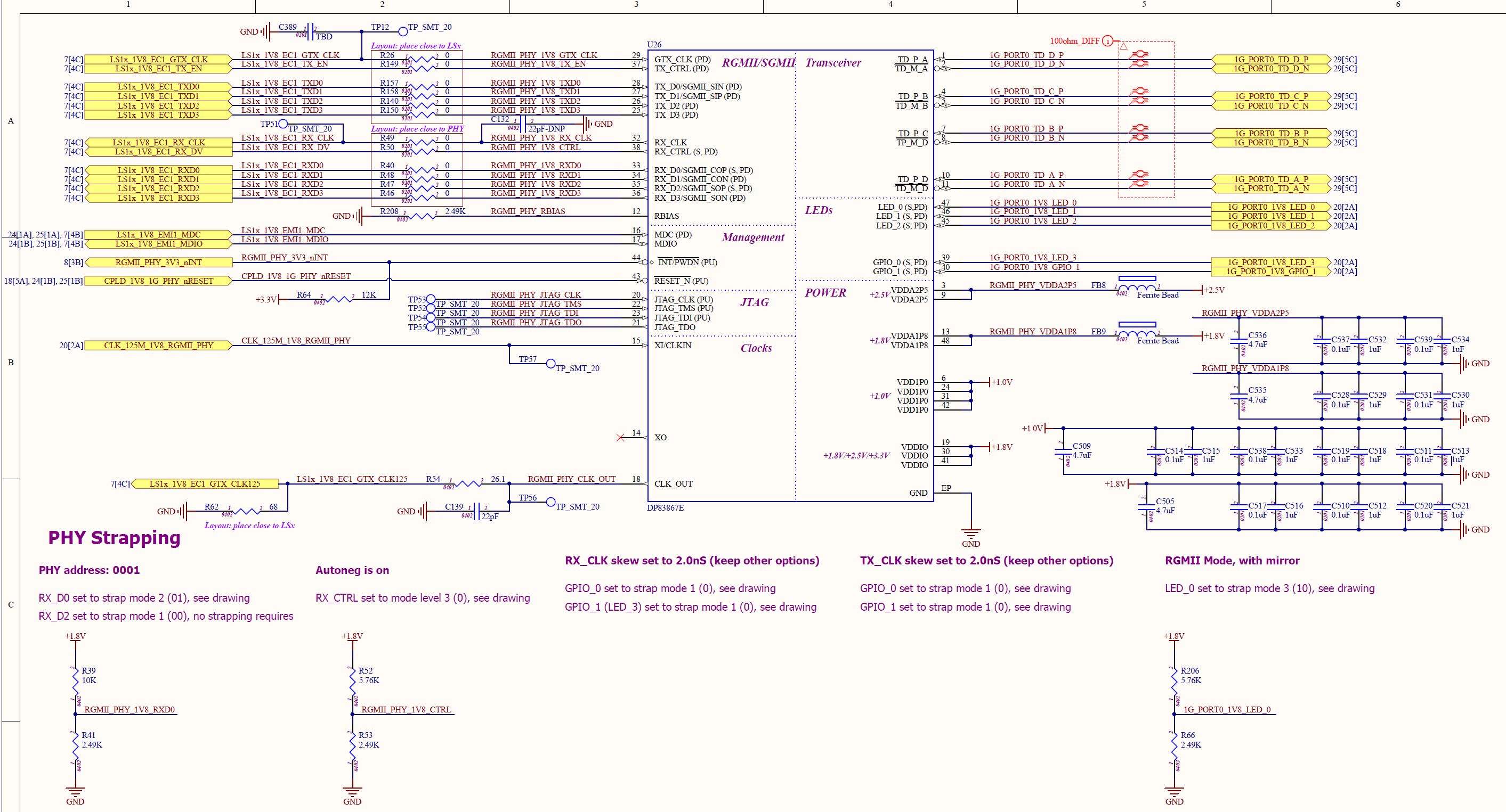
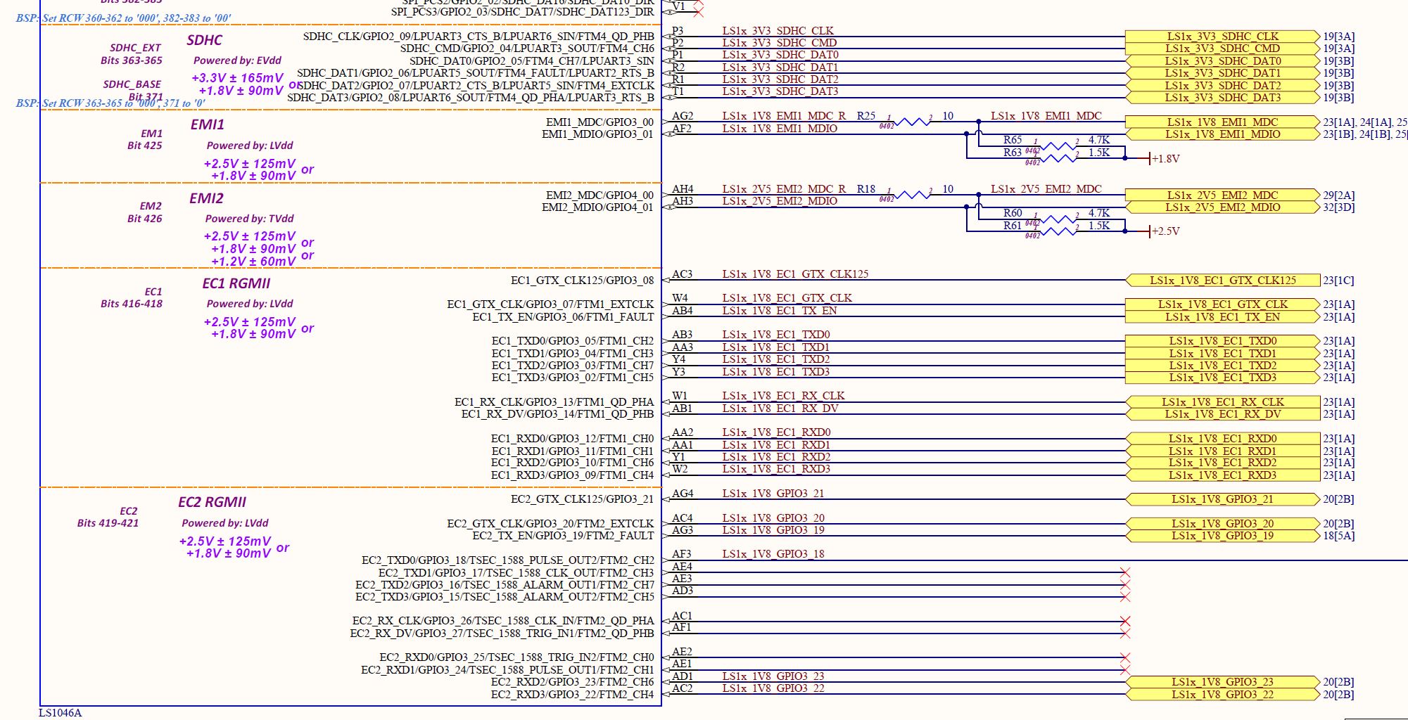
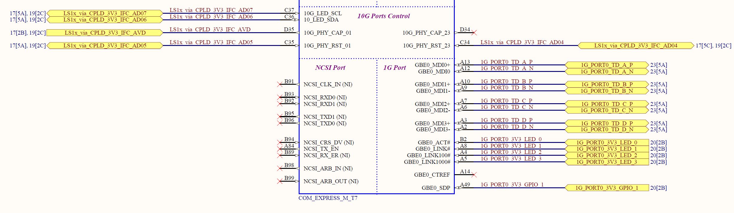
Can't seem to figure out why device is unable to function properly..  Reviewed voltage levels and clock, all appear to be within datasheet parameters.  Replaced device with new one and still same results.  Any idea what would cause such behavior? 

  • Hi Darryn,

    Do you have a schematic?

    Problems with MDIO are usually related to improper strapping. GPIO_0 can often cause this issue. If GPIO_0 is placed in mode 2 or mode 4, MDIO will become unresponsive.

    Please try to isolate GPIO_0, or pull it down strongly to ground.

    Best Regards,
  • Thank you Rob for getting back to me.  I didn't see that in the data sheet as a potential problem.

  • Hi Darryn,

    I see a few items you may want to verify and correct in your schematic if needed.

    1. RBIAS must be 11k 1%. The schematic says 2.49k. Maybe this is mismarked.
    2. The XI reference frequency to the PHY is always 25MHz. It appears maybe that the frequency is 125MHz on this line as per the net name.
    3. I don't see a pull-up resistor on MDIO, maybe it is off sheet. Please make sure there is 1 1.5k - 2.2k pull-up on MDIO net. MDIO is an open drain pin and needs a pull-up to VDDIO.

    Do you have a diagram of the LED circuit? 1.8V is a low voltage and your LEDs may not glow brightly due to the low voltage.

    Best Regards,
  • Thank you for your feedback Rob.

    RBIAS did have an incorrect resistor installed, but we caught that earlier.

    The 125MHz clock is a typo.  It is 25MHz.  

    We have three PHYs, so the 9k internal pulldown on each chip creates a 3k pull down on the signal line...correct?

  • Hey Darryn,

    Thank you for sharing the extra pages of the schematics. I still do not see the LED circuit. I want to see all connections to the 1G_PORT0_1V8_LED_3 and 1G_PORT0_1V8_GPIO_1 nets.

    Best Regards,
  • Hi Rob,

    Those two signals are being routed to a CPLD (Altera Max5) device, which is being used as a voltage translator. (+1.8V --->+3.3V).

    Their outputs go to a connector where they are unused. I'd have to review the designer's code to see if they're being driven at all.

    We contracted out this design and I'm trying to figure out the problems and solve them, so I really appreciate your help!

  • Hi Darryn,

    Can you probe those traces and hold the DP83867 in reset using the RESET_N signal? You should see 0V on those lines if you are in mode 1. Any voltage on those lines will cause the PHY to strap into an improper mode.

    If not, can you sever the traces anywhere physically on the board?

    Best Regards,
  • Sorry Rob, I misread the schematic.

  • Rob,

    I'll have to get that for you tomorrow.

    Thank you for your help.

    Darryn
  • Darryn,

    Your net names aren't matching up between the LED circuit and the schematic of the PHY you have posted earlier.

    I am asking about the LED circuit because it appears you are using a 1.8V IO and connecting the LED in the way that the PHY is sinking the current through the LED.  While this will let the LED function, it will play havoc with strap voltages when the output driver of the PHY is placed in tristate to sample the voltage on that LED pin.

    If your LED circuit looks like the one below, your straps will be going into an unknown mode.  You also have the possibility of damaging the LED driver over time if the 3.3V rail comes up before the 1.8V VDDIO is powered.  In that case, the LED pin voltage exceeds the abs max which is VDDIO + 0.3V.

    This improper mode strapping can result in the MDIO malfunction you are seeing.  The use case isn't shown in the datasheet as it has a lot of considerations for use, including improper strap mode and possible damage to the PHY.  I will be writing a TechNote about this topic because it comes up occasionally.

    The recommended LED circuits in the datasheet and EVM are designed to handle the use of LEDs when VDDIO = 1.8V in the best way possible, though it adds the cost of an external FET.  Please see datasheet section 8.5.3 LED Operation From 1.8-V I/O VDD Supply.

    You can setup the LED circuit as you may have in your schematic, but you will run into problems with straps. 

    Best Regards,

  • Hi Rob,

    The engineer working on this Ethernet PHY issue now has access to the device registers, but can't get the device to "ping" yet.

    We are having trouble in u-boot and are wondering if you have any experience using this PHY with the NXP LS1046A ARM processor?

    Thank you,

    ~Darryn

  • Hi Rob,

    We tried to ping the Ethernet PHY and received this response..

    Using FM1@DTSEC3 device
    FM1@DTSEC3: Tx error, txbd->status = 0x8800
    FM1@DTSEC3: Tx buffer not ready, txbd->status = 0x8800
    FM1@DTSEC3: Tx buffer not ready, txbd->status = 0x8800

    Thank you for any insights.

    ~Darryn
  • Hi Darryn,

    What do you mean by ping? Do you mean using the ping network command? The ping network command is a much higher level than HW and can be dependent on the system properly initializing.

    If the device is responding to MDIO, can you give me the values from registers 0x0 to 0x1f, and 0x6e and 0x6f.

    Best Regards,
  • => mdio read 1 0-1f
    1 is not a known ethernet
    Reading from bus FSL_MDIO0
    PHY at address 1:
    0 - 0x1140
    1 - 0x796d
    2 - 0x2000
    3 - 0xa231
    4 - 0x1e1
    5 - 0x4de1
    6 - 0x65
    7 - 0x2001
    8 - 0x6001
    9 - 0x200
    10 - 0xc00
    11 - 0x0
    12 - 0x0
    13 - 0x401f
    14 - 0x810
    15 - 0x3000
    16 - 0x4040
    17 - 0x7c02
    18 - 0x0
    19 - 0x9cc2
    20 - 0x29c7
    21 - 0x0
    22 - 0x0
    23 - 0x40
    24 - 0x6150
    25 - 0x4444
    26 - 0x2
    27 - 0x0
    28 - 0x0
    29 - 0x0
    30 - 0x2
    31 - 0x0

    0x6e and 0x6f is not register number
  • Hi Darryn,

    Thank you. This is very good to see. Register 0x1 bit[2] = 1 is indicating your link is up. From register 0x11(17d in your list) I see that the speed is resolved to 100M.

    Finally the output that address 0x6e and 0x6f is not a register number indicates that only clause 22 registers can be reached. The extended registers are reached by clause 22 using the indirect method. Please see section 8.4.2.1 Extended Address Space Access, and 8.4.2.1.4 Read (No Post Increment) Operation, of the datasheet.

    Best Regards,
  • HI Rob,

    We solved the issue in u-boot with the Tx errors by removing R62 and C139 (The clk out was being attenuated to 1v). Do you have an experience with u-boot?

    The ti driver (ti.c) doesn't seem to be taking the register values when we print them out. When we use the command line tool we are able to set them by hand. Is there something we are missing that we need to initialize? 

    Thanks!

  • Good afternoon Rob,

    The schematic shows that the MDI Lanes are reversed. A-->D, B-->C, C-->B, & D-->A. Does this PHY support S/W order change?

    Thank you.
  • hi darryn,

    Yes it does. The option is called mirror mode. Please enable mirror mode to reverse the order of the channels.

    Though if your order was incorrect, you'd never get a link at any speed, 10/100/1000. Your original register dump shows a link is up.

    Best Regards,
  • I understand.  Thank you Rob.

    The u-Boot driver is problematic though.  Any insight into this?

    Is there a working ARM U-Boot driver available for this device?


    Best regards,


    ~Darryn


  • Rob,

    Here are the other registers you requested.

    Dump extended Regs
    Read Reg=6e, Val=8001
    Read Reg=6f, Val=100
    Read Reg=32, Val=d3
    Read Reg=86, Val=a8
    Read Reg=170, Val=310

    Thank you,

    ~Darryn
  • Moved to direct support. HW appears to be resolved but uboot software may have issues.

    Best Regards,