This thread has been locked.

If you have a related question, please click the "Ask a related question" button in the top right corner. The newly created question will be automatically linked to this question.

LMH1983: Control flow of LMH1983

Part Number: LMH1983
Other Parts Discussed in Thread: ALP, LMK03328, LMK03328EVM

Hello team,

My customer is asking that  LMH1983's control flow and development tools.

Because this is the first time that customer uses this part and they need some useful resource.

Do you have any documents or tools that can help customer to understand this part?

Thanks.

Ben,

  • Please see the EVK user guide and ALP software GUI tool found here. The GUI can help to generate the register settings.
    www.ti.com/.../SD1983EVK

    Also refer to the datasheet for register programming details.

    Alan
  • Hello Alan,

    Thank for your reply.

    Our customer use LMK03328 that it couldn't set up the expected output.

    The system block diagram is as below.

    LMH1983 can output 27MHz normally.

    They use TI's TICS Pro tool to calculate the suitable setup as above block. The setup is as attached file.

    They also read the register of LMK03328 and the register setup is as expected but they couldn't read the expected output (always low)

    The setup flow is as below:

            // setup the LMH1983
            I2C1WriteSingle(I2cAdrsLmh, 0x05, 0x80);
            I2C1WriteSingle(I2cAdrsLmh, 0x05, 0x23);
            I2C1WriteSingle(I2cAdrsLmh, 0x09, 0x01);
      
            // setup the LMK03328
            I2C1WriteSingle(I2cAdrsLmk, 25, 0x50 );
            I2C1WriteSingle(I2cAdrsLmk, 29, 0x3f );
            I2C1WriteSingle(I2cAdrsLmk, 30, 0x00 );

            // output control set
            I2C1WriteSingle(I2cAdrsLmk, 31, 0x28 );          // OUT0
            I2C1WriteSingle(I2cAdrsLmk, 32, 0x2c );          // OUT1
            I2C1WriteSingle(I2cAdrsLmk, 34, 0xa8 );          // OUT2
            I2C1WriteSingle(I2cAdrsLmk, 35, 0x2c );          // OUT3
           
            I2C1WriteSingle(I2cAdrsLmk, 37, 0x54 );          // OUT4
            I2C1WriteSingle(I2cAdrsLmk, 39, 0x0c );          // OUT5 disable
            I2C1WriteSingle(I2cAdrsLmk, 41, 0x0c );          // OUT6 disable
            I2C1WriteSingle(I2cAdrsLmk, 43, 0x01 );          // OUT7 disable       

            I2C1WriteSingle(I2cAdrsLmk, 50, 0x5f );          // IPCLKSEL R50 (default 0x85): diff, diff, sec, sec

            I2C1Read(I2cAdrsLmk, 56, &reg, 1);
            I2C1WriteSingle(I2cAdrsLmk, 56, reg | (1<<0) );                         // PLL1 disable - to start configuring

            // DIV set
            I2C1WriteSingle(I2cAdrsLmk, 33, 0x01 );
            I2C1WriteSingle(I2cAdrsLmk, 36, 0x02 );
            I2C1WriteSingle(I2cAdrsLmk, 38, 0x02 );
            I2C1WriteSingle(I2cAdrsLmk, 40, 0x01 );
            I2C1WriteSingle(I2cAdrsLmk, 42, 0x01 );

            I2C1WriteSingle(I2cAdrsLmk, 52, 0x02 );
            I2C1WriteSingle(I2cAdrsLmk, 53, 0x00 );
            I2C1WriteSingle(I2cAdrsLmk, 57, 0x08 );
            I2C1WriteSingle(I2cAdrsLmk, 58, 0 );
            I2C1WriteSingle(I2cAdrsLmk, 59, 0x32 );

            // PLL set
            I2C1WriteSingle(I2cAdrsLmk, 56, 0x10 );
            I2C1WriteSingle(I2cAdrsLmk, 71, 0x08 );
           
            // Orther set
            I2C1WriteSingle(I2cAdrsLmk, 24, 0x00 );         
            I2C1WriteSingle(I2cAdrsLmk, 44, 0x01 );
            I2C1WriteSingle(I2cAdrsLmk, 55, 0x00 );
            I2C1WriteSingle(I2cAdrsLmk, 60, 0x00 );
            I2C1WriteSingle(I2cAdrsLmk, 61, 0x00 );
            I2C1WriteSingle(I2cAdrsLmk, 62, 0x00 );
            I2C1WriteSingle(I2cAdrsLmk, 63, 0x00 );
            I2C1WriteSingle(I2cAdrsLmk, 64, 0x00 );
            I2C1WriteSingle(I2cAdrsLmk, 65, 0x01 );
            I2C1WriteSingle(I2cAdrsLmk, 66, 0x0C );
            I2C1WriteSingle(I2cAdrsLmk, 72, 0x18 );

    LMK03328 setting.txt
    R0	0x0010
    R1	0x010b
    R2	0x0232
    R3	0x0301
    R4	0x0401
    R5	0x0500
    R6	0x0675
    R7	0x078d
    R8	0x0802
    R9	0x0900
    R10	0x0aa8
    R11	0x0b00
    R12	0x0c80
    R13	0x0d00
    R14	0x0e00
    R15	0x0f00
    R16	0x1000
    R17	0x1100
    R18	0x1200
    R19	0x1303
    R20	0x1480
    R21	0x1520
    R22	0x1600
    R23	0x1700
    R24	0x1800
    R25	0x1950
    R26	0x1a00
    R27	0x1ba0
    R28	0x1c50
    R29	0x1d3f
    R30	0x1e00
    R31	0x1f28
    R32	0x202c
    R33	0x2101
    R34	0x22a8
    R35	0x232c
    R36	0x2402
    R37	0x2554
    R38	0x2602
    R39	0x270c
    R40	0x2801
    R41	0x290c
    R42	0x2a01
    R43	0x2b00
    R44	0x2c01
    R45	0x2d80
    R46	0x2e05
    R47	0x2f00
    R48	0x3090
    R49	0x3100
    R50	0x325f
    R51	0x3300
    R52	0x3402
    R53	0x3500
    R54	0x3602
    R55	0x3700
    R56	0x3810
    R57	0x3908
    R58	0x3a00
    R59	0x3b32
    R60	0x3c00
    R61	0x3d00
    R62	0x3e00
    R63	0x3f00
    R64	0x4000
    R65	0x4101
    R66	0x420c
    R67	0x4300
    R68	0x4400
    R69	0x4500
    R70	0x4600
    R71	0x4708
    R72	0x4818
    R73	0x4900
    R74	0x4a32
    R75	0x4b00
    R76	0x4c00
    R77	0x4d00
    R78	0x4e00
    R79	0x4f00
    R80	0x5001
    R81	0x5108
    R82	0x5214
    R83	0x5300
    R84	0x5400
    R85	0x5500
    R86	0x5600
    R87	0x5700
    R88	0x5800
    R89	0x591a
    R90	0x5a00
    R91	0x5b00
    R92	0x5c00
    R93	0x5dfd
    R94	0x5e00
    R95	0x5f18
    R96	0x6001
    R97	0x611a
    R98	0x6200
    R99	0x6311
    R100	0x6400
    R101	0x650a
    R102	0x6600
    R103	0x6720
    R104	0x6800
    R105	0x6920
    R106	0x6a00
    R107	0x6b00
    R108	0x6c00
    R109	0x6d00
    R110	0x6e00
    R111	0x6f0c
    R112	0x7000
    R113	0x7100
    R114	0x7210
    R115	0x7300
    R116	0x7400
    R117	0x7580
    R118	0x7604
    R119	0x7708
    R120	0x7800
    R121	0x790a
    R122	0x7a00
    R123	0x7b00
    R124	0x7c00
    R125	0x7d00
    R126	0x7e01
    R127	0x7f04
    R128	0x8002
    R129	0x8103
    R130	0x8211
    R131	0x8380
    R132	0x8400
    R133	0x8500
    R134	0x8600
    R135	0x87a1
    R136	0x8801
    R137	0x8902
    R138	0x8a00
    R139	0x8b01
    R140	0x8c03
    R141	0x8d00
    R142	0x8eff
    R143	0x8f00
    R144	0x9018
    R145	0x9100
    R169	0xa900
    R172	0xac38
    R173	0xad2d

            I2C1WriteSingle(I2cAdrsLmk, 73, 0x00 );
            I2C1WriteSingle(I2cAdrsLmk, 74, 0x32 );
            I2C1WriteSingle(I2cAdrsLmk, 75, 0x00 );
            I2C1WriteSingle(I2cAdrsLmk, 76, 0x00 );
            I2C1WriteSingle(I2cAdrsLmk, 77, 0x00 );
            I2C1WriteSingle(I2cAdrsLmk, 78, 0x00 );
            I2C1WriteSingle(I2cAdrsLmk, 79, 0x00 );
            I2C1WriteSingle(I2cAdrsLmk, 80, 0x01 );
            I2C1WriteSingle(I2cAdrsLmk, 117, 0x80 );
            I2C1WriteSingle(I2cAdrsLmk, 120, 0x00 );

            // Reset
            I2C1WriteSingle(I2cAdrsLmk, 12, 0x00 );
            I2C1WriteSingle(I2cAdrsLmk, 12, 0x80 );

    They would like to know whether the whole setup progress is correct or not.

    Is there any other point which should notice?

  • There were several issues with the register settings.  I generated a revised configuration that matches the frequency plan in the block diagram you provided.  Both 270 MHz and 300 MHz output frequencies can be generated using single PLL1 (VCO1 = 5400 MHz), so PLL2 could be powered down.

    Please have them try the revised register export data.  I included the TICS Pro setup file (tcs) in case they want to view it graphically, and make any changes if they need.

    Alan

    LMK03328_Secref=27M_Out01=270M_Out234=300M_r1.txt
    R0	0x0010
    R1	0x010B
    R2	0x0232
    R3	0x0300
    R4	0x0400
    R5	0x0500
    R6	0x0600
    R7	0x0700
    R8	0x0800
    R9	0x0900
    R10	0x0A00
    R11	0x0B00
    R12	0x0CDF
    R13	0x0D00
    R14	0x0E00
    R15	0x0F00
    R16	0x1000
    R17	0x1100
    R18	0x1200
    R19	0x1300
    R20	0x14FF
    R21	0x15FF
    R22	0x16FF
    R23	0x1702
    R24	0x1800
    R25	0x19F5
    R26	0x1A00
    R27	0x1B18
    R28	0x1C28
    R29	0x1D0B
    R30	0x1E78
    R31	0x1F28
    R32	0x2028
    R33	0x2109
    R34	0x2228
    R35	0x2328
    R36	0x2408
    R37	0x2514
    R38	0x2608
    R39	0x2700
    R40	0x2802
    R41	0x2900
    R42	0x2A05
    R43	0x2B00
    R44	0x2C05
    R45	0x2D0A
    R46	0x2E00
    R47	0x2F00
    R48	0x30FF
    R49	0x3100
    R50	0x326F
    R51	0x3303
    R52	0x3400
    R53	0x3500
    R54	0x3600
    R55	0x3700
    R56	0x3806
    R57	0x3918
    R58	0x3A00
    R59	0x3B64
    R60	0x3C00
    R61	0x3D00
    R62	0x3E00
    R63	0x3F00
    R64	0x4000
    R65	0x4101
    R66	0x420C
    R67	0x4308
    R68	0x4401
    R69	0x4504
    R70	0x4607
    R71	0x4703
    R72	0x4818
    R73	0x4900
    R74	0x4A64
    R75	0x4B00
    R76	0x4C00
    R77	0x4D00
    R78	0x4E00
    R79	0x4F00
    R80	0x5001
    R81	0x510C
    R82	0x5204
    R83	0x5301
    R84	0x5404
    R85	0x5507
    R86	0x5600
    R87	0x5700
    R88	0x5800
    R89	0x59DE
    R90	0x5A01
    R91	0x5B18
    R92	0x5C01
    R93	0x5D4B
    R94	0x5E01
    R95	0x5F86
    R96	0x6001
    R97	0x61BE
    R98	0x6201
    R99	0x63FE
    R100	0x6402
    R101	0x6547
    R102	0x6602
    R103	0x679E
    R104	0x6800
    R105	0x6900
    R106	0x6A05
    R107	0x6B0F
    R108	0x6C0F
    R109	0x6D0F
    R110	0x6E0F
    R111	0x6F00
    R112	0x7000
    R113	0x7100
    R114	0x7200
    R115	0x7308
    R116	0x7419
    R117	0x7500
    R118	0x7607
    R119	0x7705
    R120	0x7800
    R121	0x790F
    R122	0x7A0F
    R123	0x7B0F
    R124	0x7C0F
    R125	0x7D00
    R126	0x7E00
    R127	0x7F00
    R128	0x8000
    R129	0x8108
    R130	0x8219
    R131	0x8300
    R132	0x8407
    R133	0x8505
    R134	0x8600
    R135	0x8700
    R136	0x8800
    R137	0x8910
    R138	0x8A00
    R139	0x8B00
    R140	0x8C00
    R141	0x8D00
    R142	0x8E00
    R143	0x8F00
    R144	0x9000
    R145	0x9100
    R169	0xA940
    R172	0xAC24
    R173	0xAD00
    

    LMK03328_Secref=27M_Out01=270M_Out234=300M_r1.tcs

  • Alan,

    They tried the parameters provided by you.
    And they still couldn't get any clock from LMK03328

    There are few questions from customer

    • Is there a register that can confirm whether the input frequency is stable or not?
    • Attach the LMH1983 output to the LMK03328 waveform. Is the output waveform correct?
    • Attached their current schematic, and please help to check the current schematic

    Thank for your help.

     ?

  • In the register setting I provided, I configured STATUS0 to SECREF Loss of Signal (LOS) and STATUS1 to PLL1 Loss of Lock (LOL), with both active high.  If SECREF is detected and PLL1 is locked, then both STATUS pins should output logic 0.

    Thanks for sharing the schematic.  I noticed the GPIO0 (SYNCN, active low) input pin is open.  So, it is possible the outputs are muted because output SYNC is asserted (GPIO0 pin is pulled down internally), since my register setting has PLL1_SYNC_EN = 1 which causes PLL1 output to muted when output SYNC is asserted.

    Can they try changing PLL1_SYNC_EN = 0 (write 0x04 to Register 0x38), and check if the outputs are toggling (not muted)?

    Regards,
    Alan

  • LMK03328_Secref=27M_Out01=270M_Out24=300M_r2.7zHello Alan,

    The customer has used the attached setup to test the board.

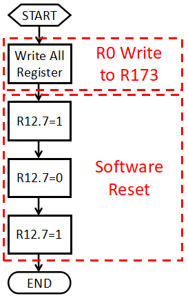
    This test is to directly write the register R0 to the end, and at the end there is a software register.

    But they still couldn't get the output signal of LMK03328.

    Can I apply a EVM for them or could you help to write the current settings to the LMK03328 EVM to see if it works as expected?

    If the LMK03328 EVM can operate normally, the bug is more hardware-oriented.

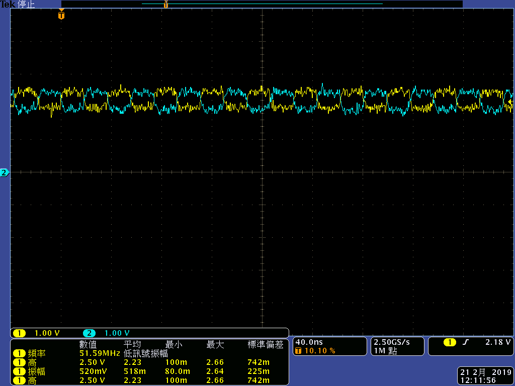
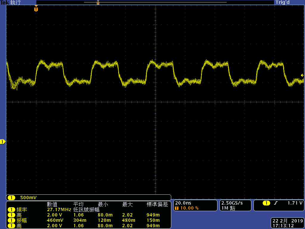
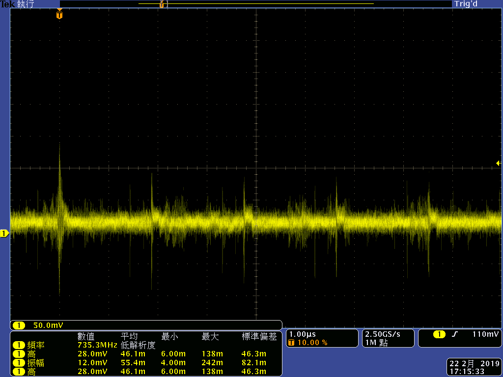
    Attached this measurement waveform.

    Input of LMK03328


    Output of LMK03328

  • Hello,

    I am travelling this week but have asked a colleague to try this config file on a LMK03328EVM.

    Thanks,
    Alan
  • Hello Alan,

    Thank for your help. Looking forward your colleague's reply.

    Best Regards

    Ben
  • Hi Ben,

    I was able to successfully generate an output using these settings.
    You may need to issue a software reset by toggling the RESETN_SW bit.

    To debug it, first check the STATUS outputs. STATUS0 is configured to SECREF Loss of Signal (LOS), and STATUS1 is configured to PLL1 Loss of Lock (LOL), with both active high. If SECREF is detected and PLL1 is locked, then both STATUS pins should output logic 0.

    Kind regards,
    Lane
  • Hello Lane & Alan,

    The customer's reset control process is as below. Is there any wrong about it?

    LMK03328_Register.txt
    R0	0x0010
    R1	0x010b
    R2	0x0232
    R3	0x0301
    R4	0x0401
    R5	0x0500
    R6	0x0675
    R7	0x0719
    R8	0x0802
    R9	0x0900
    R10	0x0aa8
    R11	0x0b00
    R12	0x0cdf
    R13	0x0d00
    R14	0x0e00
    R15	0x0f00
    R16	0x1000
    R17	0x1100
    R18	0x1200
    R19	0x1300
    R20	0x14ff
    R21	0x15ff
    R22	0x16ff
    R23	0x1702
    R24	0x1800
    R25	0x19f5
    R26	0x1a00
    R27	0x1b20
    R28	0x1c50
    R29	0x1d02
    R30	0x1e78
    R31	0x1f28
    R32	0x2028
    R33	0x2109
    R34	0x2228
    R35	0x2300
    R36	0x2408
    R37	0x2514
    R38	0x2608
    R39	0x2700
    R40	0x2802
    R41	0x2900
    R42	0x2a05
    R43	0x2b00
    R44	0x2c05
    R45	0x2d0a
    R46	0x2e00
    R47	0x2f00
    R48	0x30ff
    R49	0x3100
    R50	0x326f
    R51	0x3303
    R52	0x3400
    R53	0x3500
    R54	0x3600
    R55	0x3700
    R56	0x3804
    R57	0x3918
    R58	0x3a00
    R59	0x3b64
    R60	0x3c00
    R61	0x3d00
    R62	0x3e00
    R63	0x3f00
    R64	0x4000
    R65	0x4101
    R66	0x420c
    R67	0x4308
    R68	0x4401
    R69	0x4504
    R70	0x4607
    R71	0x4703
    R72	0x4818
    R73	0x4900
    R74	0x4a64
    R75	0x4b00
    R76	0x4c00
    R77	0x4d00
    R78	0x4e00
    R79	0x4f00
    R80	0x5001
    R81	0x510c
    R82	0x5204
    R83	0x5301
    R84	0x5404
    R85	0x5507
    R86	0x5600
    R87	0x5700
    R88	0x5800
    R89	0x59de
    R90	0x5a01
    R91	0x5b18
    R92	0x5c01
    R93	0x5d4b
    R94	0x5e01
    R95	0x5f86
    R96	0x6001
    R97	0x61be
    R98	0x6201
    R99	0x63fe
    R100	0x6402
    R101	0x6547
    R102	0x6602
    R103	0x679e
    R104	0x6800
    R105	0x6900
    R106	0x6a05
    R107	0x6b0f
    R108	0x6c0f
    R109	0x6d0f
    R110	0x6e0f
    R111	0x6f00
    R112	0x7000
    R113	0x7100
    R114	0x7200
    R115	0x7308
    R116	0x7419
    R117	0x7500
    R118	0x7607
    R119	0x7705
    R120	0x7800
    R121	0x790f
    R122	0x7a0f
    R123	0x7b0f
    R124	0x7c0f
    R125	0x7d00
    R126	0x7e00
    R127	0x7f00
    R128	0x8000
    R129	0x8108
    R130	0x8219
    R131	0x8300
    R132	0x8407
    R133	0x8505
    R134	0x8600
    R135	0x8777
    R136	0x8802
    R137	0x8912
    R138	0x8a00
    R139	0x8b00
    R140	0x8c00
    R141	0x8d02
    R142	0x8eff
    R143	0x8f00
    R144	0x9000
    R145	0x9100
    R169	0xa940
    R172	0xac24
    R173	0xad00
    

    The attached txt file is what we read from the customer register.

    R27 >>0x1b20   STAT0_POL=0 means STATUS0 is active low.

    And, we read the status0,1 as below table. Does it mean that we didn't receive ref signal correctly?

    Thank for your help.

  • If STATUS0 is active low, the results in the table indicate that:
    -PRIREF and SECREF are detected
    -the PLLs are locked

    Based on these results, I would expect a valid clock output. Make sure you have the appropriate termination network. For CML, the termination shown in datasheet Figure 67 is valid.

    Kind regards,
    Lane