This thread has been locked.

If you have a related question, please click the "Ask a related question" button in the top right corner. The newly created question will be automatically linked to this question.

DS90UB949-Q1: We want the EDID stored in EEPROM to be loaded to SRAM of serializer but we are able to see Internal pre-programmed EDID in the SRAM. This shows EDID stored in EEPROM is not loaded to SRAM.

Part Number: DS90UB949-Q1
Other Parts Discussed in Thread: ALP

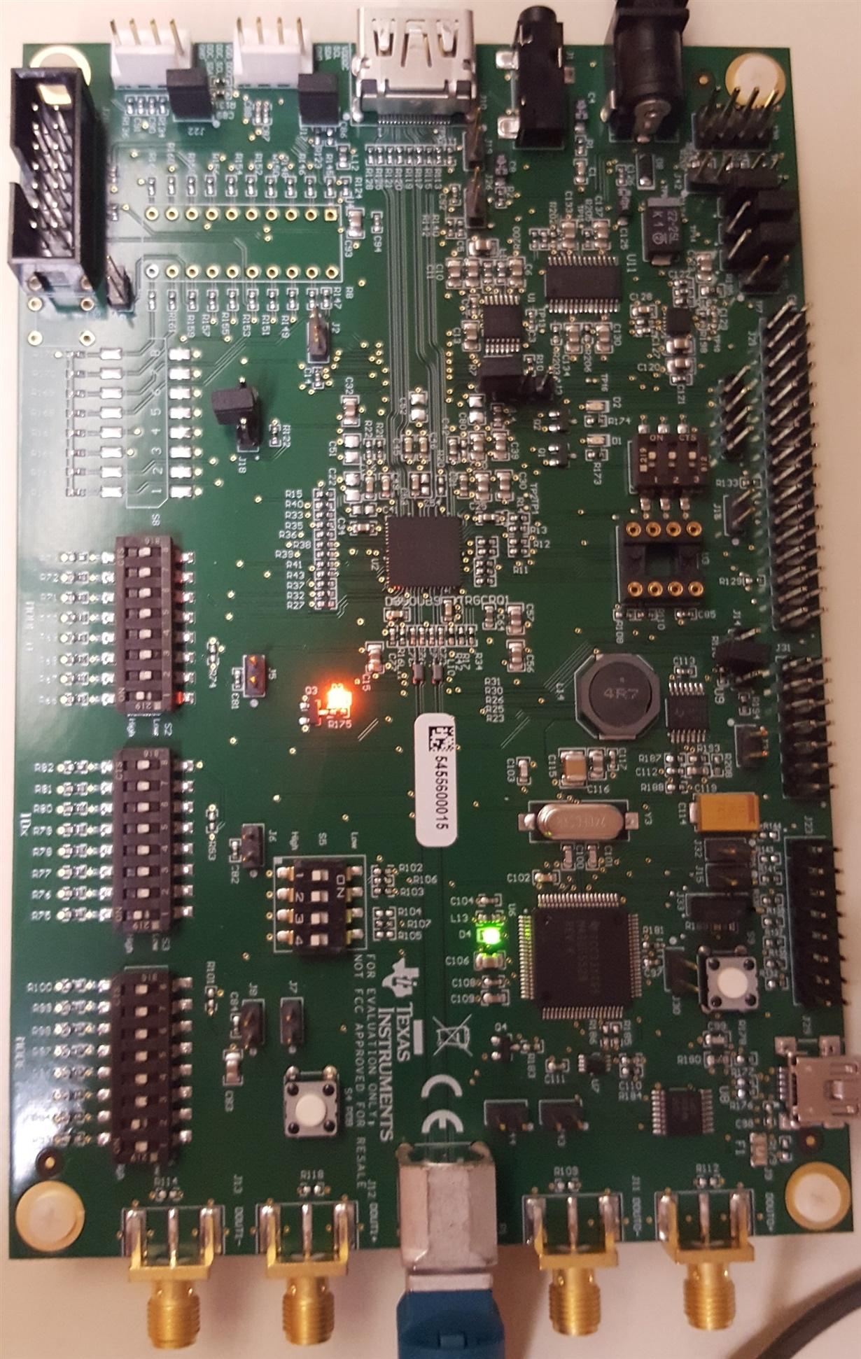
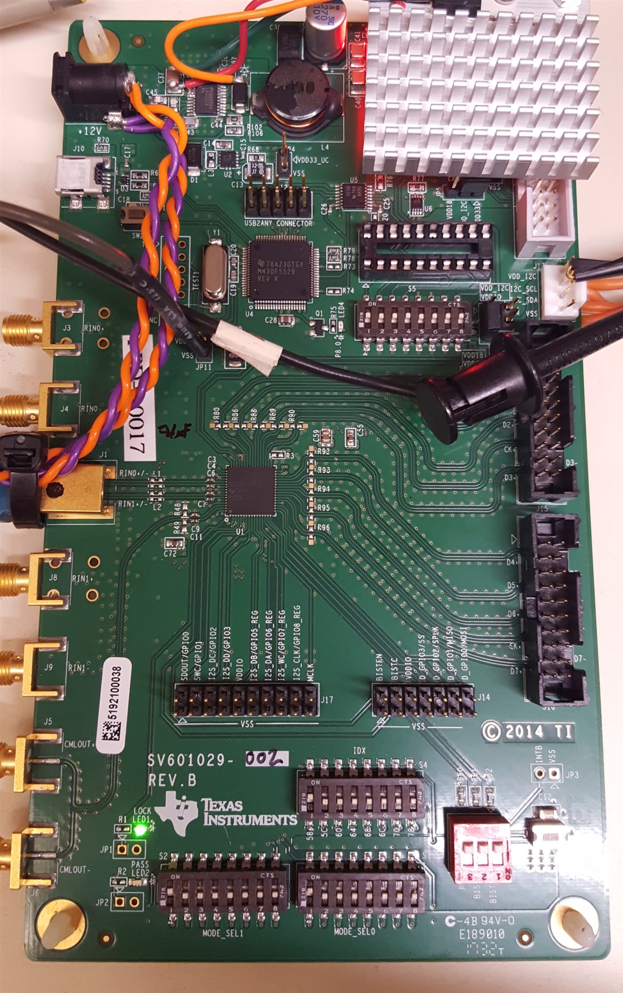
We are using serializer DS90UB949 evm and our deserializer to which EEPROM is connected with 0x50 (7 bit) address.

Issue: We want the EDID stored in EEPROM to be loaded to SRAM of serializer but we are able to see Internal pre-programmed EDID in the SRAM. This shows EDID stored in EEPROM is not loaded to SRAM.

Mode select configuration settings:

We are keeping MODE_SEL0 as 1 and MODE_SEL1 as 4 for External remote EDID configuration.

Below are the register dump of serializer(0x0c) and deserializer(0x2c),

=====================================================

msm8996:/data # ./i2cdump -f -y 8 0x0c

./i2cdump -f -y 8 0x0c

No size specified (using byte-data access)

     0  1  2  3  4  5  6  7  8  9  a  b  c  d  e  f    0123456789abcdef

00: 18 00 00 da 80 00 58 50 50 00 04 00 07 25 30 03    ?..??.XPP.?.?%0?

10: 00 00 00 a8 00 00 fe 1e 7f 7f 01 00 00 00 01 00    ...?..?????...?.

20: 0b 00 25 00 00 00 00 00 01 20 20 a0 00 00 a5 5a    ?.%.....?  ?..?Z

30: 00 00 00 00 00 00 00 00 00 00 00 00 00 00 00 00    ................

40: 14 55 00 00 80 00 00 00 00 00 00 00 00 00 00 00    ?U..?...........

50: 97 a0 1e 00 28 0c 00 00 00 00 dd a0 02 06 44 48    ???.(?....????DH

60: 22 02 00 00 10 00 00 00 00 00 00 00 00 00 00 00    "?..?...........

70: 78 28 a0 00 00 00 00 78 28 a0 00 00 00 00 00 00    x(?....x(?......

80: 00 00 00 00 00 00 00 00 00 00 00 00 00 00 00 00    ................

90: 00 00 00 00 00 00 00 00 00 00 00 00 00 00 00 00    ................

a0: 00 00 00 00 00 00 00 00 00 00 00 00 00 00 00 00    ................

b0: 00 00 00 00 00 00 00 00 00 00 00 00 00 00 00 00    ................

c0: 00 00 a8 00 28 00 00 60 c0 00 00 00 00 00 ff 00    ..?.(..`?.......

d0: 00 00 00 00 00 00 00 00 00 00 00 00 00 00 00 00    ................

e0: 00 00 a8 00 28 38 00 00 00 00 00 00 00 00 00 00    ..?.(8..........

f0: 5f 55 42 39 34 39 00 00 00 00 00 00 00 00 00 00    _UB949..........

msm8996:/data #

msm8996:/data #

msm8996:/data # ./i2cdump -f -y 8 0x2c

./i2cdump -f -y 8 0x2c

No size specified (using byte-data access)

     0  1  2  3  4  5  6  7  8  9  a  b  c  d  e  f    0123456789abcdef

00: 58 04 00 f0 fe 1e 00 18 00 00 00 00 00 00 00 00    X?.???.?........

10: 00 00 00 00 00 00 00 00 00 01 00 00 0b 13 50 05    .........?..??P?

20: 00 00 40 28 08 00 83 84 01 00 00 00 00 00 00 00    ..@(?.???.......

30: 00 00 90 25 01 00 00 9e 00 00 00 01 20 e0 23 00    ..?%?..?...? ?#.

40: 43 03 03 00 60 88 00 00 0f 82 00 08 00 00 63 00    C??.`?..??.?..c.

50: 03 10 00 01 80 00 00 00 00 7f 20 20 00 00 00 00    ??.??....?  ....

60: 00 00 00 00 10 00 00 00 00 00 00 00 00 00 00 00    ....?...........

70: 00 00 00 07 07 08 00 00 00 00 00 5d 02 00 00 00    ...???.....]?...

80: 00 00 00 00 00 00 00 00 00 00 00 00 00 00 00 00    ................

90: 00 00 00 00 00 00 00 00 00 00 00 00 00 00 00 00    ................

a0: 00 00 8c 00 00 00 00 00 00 00 00 00 00 00 00 00    ..?.............

b0: 00 00 00 00 00 00 00 00 00 00 00 00 00 00 00 00    ................

c0: 00 00 00 00 00 00 00 00 c0 00 00 00 00 00 00 00    ........?.......

d0: 00 00 00 00 00 00 00 00 00 00 00 00 00 00 00 00    ................

e0: 00 00 00 00 00 00 00 00 00 00 00 00 00 00 00 00    ................

f0: 5f 55 42 39 34 38 00 00 00 00 00 00 00 00 00 00    _UB948..........

msm8996:/data #

=========================================================


Below is the 0x4f register settings of serializer taken from the datasheet,

From this we can see 0x4f[0] is Read only and all other are RW bits, but we could able to write to 0x4f[0][3][4] bits and could not write to 0x4f[1][2] bits.


We have done some other experiments as well to make sure other EDID configuration supported are working fine. Below are the experiment results,

Exp1: Connecting EEPROM to DDC I2C:

1.       External local EDID (EEPROM): We are able to read the EDID stored in EEPROM from the “/sys/devices/virtual/graphics/fb1/edid_raw_data” node, in the hex format.

2.       Internal EDID (SRAM): We are able to read the EDID stored in EEPROM from the “/sys/devices/virtual/graphics/fb1/edid_raw_data” and “/sys/devices/virtual/graphics/fb1/edid” nodes, in the ascii format.


In both the cases we are able to read some portion of the EDID, not the complete 256 bytes what we wrote on EEPROM.


Exp2: Connecting EEPROM to I2C (BLSP_8):

1.       External local EDID (EEPROM): We are not able to read any edid from the “edid” or “edid_raw_data” nodes.

2.       Internal EDID (SRAM): We are able to read the Internal Pre-programmed EDID in this case.

 Could you please us debug this issue?

  • Hi Pradeep, looking at it and hope to have a response Thursday.
  • Hi Mike Leister,

    We are waiting for your response.
  • Hi Prabhu,

    0x4F(1) clears itself after the EDID read. Can you set up a logic/I2C analyzer on the DDC I2C clock/data, set serializer 0x4F(1), and capture the transfer of the EDID from the EEPROM to the deserializer?
    • If the full 256 byte EDID does not transmit from the EEPROM accurately, check that the EEPROM is programmed correctly and can be fully and correctly read with another device. It sounds like you have already done this in EXP1.
    • After setting 0x4F(1), poll 0x50(4) until it goes high. Do not run any code until the EDID transfer is complete. This will make sure you are not cutting off the EDID transfer before completion.
    • If the EEPROM is transmitting the full 256 bytes and the previous step does not allow full EDID transfer, experiment with the serializer 0x52 and 0x53 registers. These tune the DDC I2C link.

    If none of this works, please do the EDID transfer 10 times and record how many bytes correctly transfer each time.

    Mike
  • Hello,

    We are able to see 0 on 0x4F(1) bit even after writing 1 to 0x4F(1). We are not able to set 0x4F(1) bit. And 0x50 register has 0x97 value ( 0x50(3) = REM_EDID_LOAD is 0).

    According to data sheet, 0x4F(0) is Read only bit and 0x4F(1)(2) are R/W. But we can set 0x4F(0), not 0x4F(1)(2). Is there any reason for this?

    We noticed below thing when we tried setting 0x4F register,

    We have set 0x54 register to 0x00. But after writing to 0x4F register, 0x54 got set to 0x28.

    Value 0x28 on 0x54 register shows Remote EDID load is disabled ( 0x54(5) = DIS_REM_EDID is set to 1). Is there any particular reason for this?


    Thank you,

    Prathibha

  • Hi Prathibha,


    Here is the 0x4F(1) sequence:

    1. You set 0x4F(1) in the serializer
    2. The serializer connects to the deserializer and kicks off DDC communication between the deserializer and the EEPROM
    3. EDID is transferred from the EEPROM to the deserializer then to the serializer and is stored in the serializer SRAM
    4. The serializer resets 0x4F(1)

    If you read 0x4F(1) after setting it but before the 256 bytes are transferred, you may see a 1.  Otherwise you will see a 0 because the serializer resets that bit when EDID load from EEPROM is complete..

    Register 0x54 should not be loaded with 0x28.  0x00 is correct.  I assume you did not program 0x54 register.

    After you set 0x4F(1), do you see the full 256 bytes come out of the EEPROM?

    Mike

  • Hello Mike,

    We have DDC i2c lines only on the serializer side. There is no DDC communication between deserializer and the EEPROM.

    We have only i2c communication between deserializer and EEPROM. EEPROM is connected to i2c_8 (BLSP_8) and Serializer/deserializer is also connected on the same i2c line.

    We are setting the 0x4F(1) bit to 1 and in the very next moment we are reading back this register, we don't see 0x4F(1) bit is set to 1.

    Just to make sure what are all bits are getting set in this 0x4F register, we wrote 0xFF to 0x4F. In the very next moment we read 0x4F register and the value was 0x19. From this experiment we see, 0x4F(1)(2) are not set and 0x4F(0) is set. This is not correct according to the datasheet explanation. Is there any reason for this? or, how can we read 0x4F before serializer resets this register?

    Just after device boot, we read 0x28 in register 0x54, hence we programed this register to 0x00 in serializer driver. But whenever we are setting 0x4F register, 0x54 register is resetting to 0x28.

    Thank you,

    Prathibha


  • Hello Mike,

    Any inputs for this?

  • Hi Prathibha,

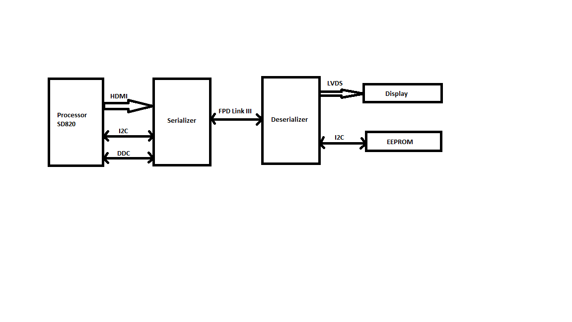
    I thought the EEPROM was in the display on the deserializer side.  That may explain the 0x4F behavior.  Can you send a block diagram?

    Mike

  • Hello

    Please find the attached document for block diagram.

    Here, we are storing EDID data in EEPROM and we want that EDID data to be loaded to SRAM of serializer.

    Thank you,

    Prathibha

  • Thanks Prathibha,

    This is good, you are configured the way EDID --> SRAM is designed to work.

    Please verify the EEPROM has the whole EDID using your programming tool.

    Please set up an oscilloscope or serial port analyzer to capture the EEPROM-Deserializer DDC bus, set 0x4F(1), and capture the 256-byte transfer.  There are several possible outcomes:

    • The whole EDID is transferred to the deserializer and the next step is to see how much of it made it to the SRAM
    • Part of the EDID transferred correctly, and part was corrupted
    • Part of the EDID transferred correctly, then the transaction stopped
    • Other?

    Please let me know the result.

    Can you send a programmed EEPROM so that I can replicate your setup?

    Michael Leister c/o Texas Instruments

    2900 Semiconductor Dr

    Santa Clara CA 95051

    Mike

  • Hello Mike,

    We tried to capture the EEPROM-Deserializer I2C lines to check if there is any data transfer between EEPROM to Deserializer. But we could not see any data on I2C lines.

    We tried setting 0x4F(1) bit to 1 and capture the EEPROM-Deserializer I2C lines but when we read back the 0x4F(1), it was 0. 

    Result: We could not see any data on I2C lines and also 0x4F(1) bit was 0 even after setting it to 1.

    Please clarify us on which DDC bus you are talking about between EEPROM-Desializer. Because we have only I2C lines (Pin number 45 and 46 of deserializer) connected between EEPROM-Deserializer.

    Thank you,

    Prathibha

  • Hello Mike,

    Any updates on this?

  • Hi Prathibha,

    I see that 949 0x50(4) is high, which is good.  You must test for this before setting 0x4F(1).

    You mentioned that the EEPROM 7-bit address is 0x50.  In that case, you must write 0x50 to 949 register 0x51(7-1).  You have it programmed to 0xA0 so the 948 is looking for the EEPROM at that address.

    949 0x50(3) is low.  This must be high before reading the SRAM.

    949 0x54(5) is preventing remote EDID read.  Check the MODE_SEL_0 and MODE_SEL_1 strapping, it looks like you have it strapped differently than reported.  This bit needs to be low.

    Mike

  • You are correct, the deserializer to EEPROM bus is I2C.

    Mike

  • Hello Mike,

    TI: You mentioned that the EEPROM 7-bit address is 0x50.  In that case, you must write 0x50 to 949 register 0x51(7-1).  You have it programmed to 0xA0 so the 948 is looking for the EEPROM at that address.

    Replay: 0x50 7-bit address is programed in 949 register 0x51(7-1), but as 0x51(0) bit is set to 0, you are able to read 0x51 register as 0xA0 (please refer to 949 datasheet Register Maps).

    TI: 949 0x50(3) is low.  This must be high before reading the SRAM.

    Replay: Yes, this 0x50(3) bit has to go high to indicate EDID SRAM has been loaded from remote EDID EEPROM. Can we know the reason, why this bit is not setting to high?

    TI: 949 0x54(5) is preventing remote EDID read.  Check the MODE_SEL_0 and MODE_SEL_1 strapping, it looks like you have it strapped differently than reported.  This bit needs to be low.

    Replay: MODE_SEL_0 is set to 1 and MODE_SEL_1 is set to 4 to select the Remote EDID configuration. If we are setting MODE_SEL_1 as 4, 0x54(5) should not be set to 1. But still this bit was going high hence we programed 0x54 register to 0x00 in kernel.

    If we are setting 0x4F register, 0x54(5) bit is getting set to 1 (0x54 set 0x28) as we have already asked this in previous posts. Can we know the reason for this?

    Thank you,

    Prathibha


  • Hello Mike,

    Any updates?

  • Hi Prathibha,

    Watch for an email setting up a debug call early next week.  I'm hoping it can be a working session where you have access to the setup.

    Mike

  • Hi Prathiba,

    I noticed that 949 register 0x54 is 0x28 or 00101000b so bit 5 is 1.  From the 949 datasheet Table 10, bit 5: "If this bit is set to a 1, the remote EDID load will be bypassed."

    Please change MODE_SEL1 from 4 to 3.

    Mike

  • Hello Mike,

    Yes, 949 register 0x54 bit 5 should not be 1. But even though we are setting MODE_SEL1 to 4 or 3, register 0x54 bit 5 is setting to 1 only.

    To make 0x54(5) bit as 0, we are writing 0x00 to register 0x54 in the kernel serializer driver file as we already mentioned in our previous comments.

    Can we know why are you suggesting us to set MODE_SEL1 to 3?  Because, if we are setting MODE_SEL1 to 3, the REM_EDID_LOAD option becomes 0. 

    Making REM_EDID_LOAD option to 0 means "Use internal SRAM EDID".  But our aim is to load the EDID from remote EEPROM to SRAM of serializer.

    Detailed explanation can be found in datasheet under section "7.4.1  Mode Select Configuration Settings (MODE_SEL[1:0])". 

    Thank you,

    Prathibha

  • Hi Prathibha,

    Interesting; 0x54(5) description appears to conflict with Table 6.

    "Disable Remote EDID load: Disables automatic load of EDID SRAM from a remote EDID

    EEPROM. By default, the device will check the remote I2C bus for an EEPROM with a

    valid EDID, and load the EDID data to local EDID SRAM. If this bit is set to a 1, the

    remote EDID load will be bypassed. This value is loaded from the MODE_SEL1 pin at

    power-up."

    In datasheet table 6, if REM_EDID_LOAD is high, "If available, remote EDID is copied into internal SRAM EDID."

    I see from your register dump that the bit is cleared, so EDID load should work.  I'll ask the FAE to set up a phone debug session with myself and a 94x expert so we can get to the bottom of this.

    Mike

  • Hello Mike,

    We tested with two case. Once by setting MODE_SEL1 to 3 and another time by setting MODE_SEL1 to 4. In both the scenario, we are able to read 0x54 register as 0x28 and 0x50 register as 0x97 only.

    Please find the below register dump of serializer in both the scenario 

    ====================================================

    MODE_SELl1 = 3
    =========================
    msm8996:/ # ./data/i2cdump -f -y 8 0x0c
    ./data/i2cdump -f -y 8 0x0c
    No size specified (using byte-data access)
         0  1  2  3  4  5  6  7  8  9  a  b  c  d  e  f    0123456789abcdef
    00: 18 00 00 da 80 00 58 50 50 00 10 00 07 25 35 03    ?..??.XPP.?.?%5?
    10: 00 00 00 a8 00 00 fe 1e 7f 7f 01 00 0c 00 01 00    ...?..?????.?.?.
    20: 0b 00 25 00 00 00 00 00 01 20 20 a8 00 00 a5 5a    ?.%.....?  ?..?Z
    30: 00 00 00 00 00 00 00 00 00 00 00 00 00 00 00 00    ................
    40: 14 55 00 00 80 00 00 00 08 00 00 00 00 00 00 00    ?U..?...?.......
    50: 97 a0 1e 00 28 0c 15 00 00 00 dd a0 02 06 44 48    ???.(??...????DH
    60: 22 02 00 00 10 00 00 00 00 00 00 00 00 00 00 00    "?..?...........
    70: 78 ba a0 00 00 00 00 78 ba a0 00 00 00 00 00 00    x??....x??......
    80: 00 00 00 00 00 00 00 00 00 00 00 00 00 00 00 00    ................
    90: 00 00 00 00 00 00 00 00 00 00 00 00 00 00 00 00    ................
    a0: 00 00 00 00 00 00 00 00 00 00 00 00 00 00 00 00    ................
    b0: 00 00 00 00 00 00 00 00 00 00 00 00 00 00 00 00    ................
    c0: 00 00 a8 00 28 38 00 00 c0 00 00 00 00 00 ff 00    ..?.(8..?.......
    d0: 00 00 00 00 00 00 00 00 00 00 00 00 00 00 00 00    ................
    e0: 00 00 a8 00 28 38 00 00 00 00 00 00 00 00 00 00    ..?.(8..........
    f0: 5f 55 42 39 34 39 00 00 00 00 00 00 00 00 00 00    _UB949..........
    msm8996:/ #

    MODE_SELl1 = 4
    =========================
    msm8996:/ # ./data/i2cdump -f -y 8 0x0c
    ./data/i2cdump -f -y 8 0x0c
    No size specified (using byte-data access)
         0  1  2  3  4  5  6  7  8  9  a  b  c  d  e  f    0123456789abcdef
    00: 18 00 00 da 80 00 58 50 50 00 03 00 07 25 35 03    ?..??.XPP.?.?%5?
    10: 00 00 00 a8 00 00 fe 1e 7f 7f 01 00 0c 00 01 00    ...?..?????.?.?.
    20: 0b 00 25 00 00 00 00 00 01 20 20 a0 00 00 a5 5a    ?.%.....?  ?..?Z
    30: 00 00 00 00 00 00 00 00 00 00 00 00 00 00 00 00    ................
    40: 14 55 00 00 80 00 00 00 08 00 00 00 00 00 00 00    ?U..?...?.......
    50: 97 a0 1e 00 28 0c 00 00 00 00 dd a0 02 06 44 49    ???.(?....????DI
    60: 22 02 00 00 10 00 00 00 00 00 00 00 00 00 00 00    "?..?...........
    70: 78 ba a0 00 00 00 00 78 ba a0 00 00 00 00 00 00    x??....x??......
    80: 00 00 00 00 00 00 00 00 00 00 00 00 00 00 00 00    ................
    90: 00 00 00 00 00 00 00 00 00 00 00 00 00 00 00 00    ................
    a0: 00 00 00 00 00 00 00 00 00 00 00 00 00 00 00 00    ................
    b0: 00 00 00 00 00 00 00 00 00 00 00 00 00 00 00 00    ................
    c0: 00 00 a8 00 28 00 00 60 c0 00 00 00 00 00 ff 00    ..?.(..`?.......
    d0: 00 00 00 00 00 00 00 00 00 00 00 00 00 00 00 00    ................
    e0: 00 00 a8 00 28 38 00 00 00 00 00 00 00 00 00 00    ..?.(8..........
    f0: 5f 55 42 39 34 39 00 00 00 00 00 00 00 00 00 00    _UB949..........
    msm8996:/ #
    Thank you,
    Prathibha
  • Hi Prathibha,

    I got an EEPROM and soldered it to my 948 EVM I2C bus.  If the system is configured as described below, the EDID loads at power-up without any intervention or register programming.

    Here is the sequence I followed that loaded the remote EEPROM:

    • Set MODE_SEL0 and MODE_SEL1 resistors so that the following 949 register bits will be zero.
      • 0x54 bit 7 = 0 Allows internal bridge control to function
      • 0x54 bit 5 = 0 Remote EDID load enabled when low
      • 0x5B bit 7 = 0 This is the setting for STP cable.  If you use coax, it should be 1.
      • 0x4F bit 0 = 0 Enables EDID access via DDC/I2C when set low.  I've filed a ticket to get the datasheet clarified.
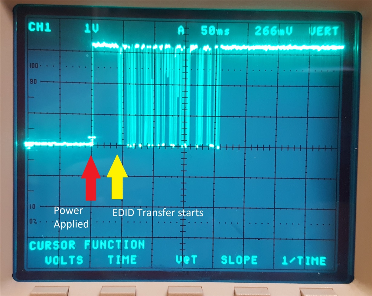
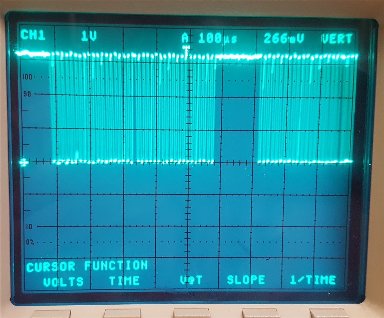
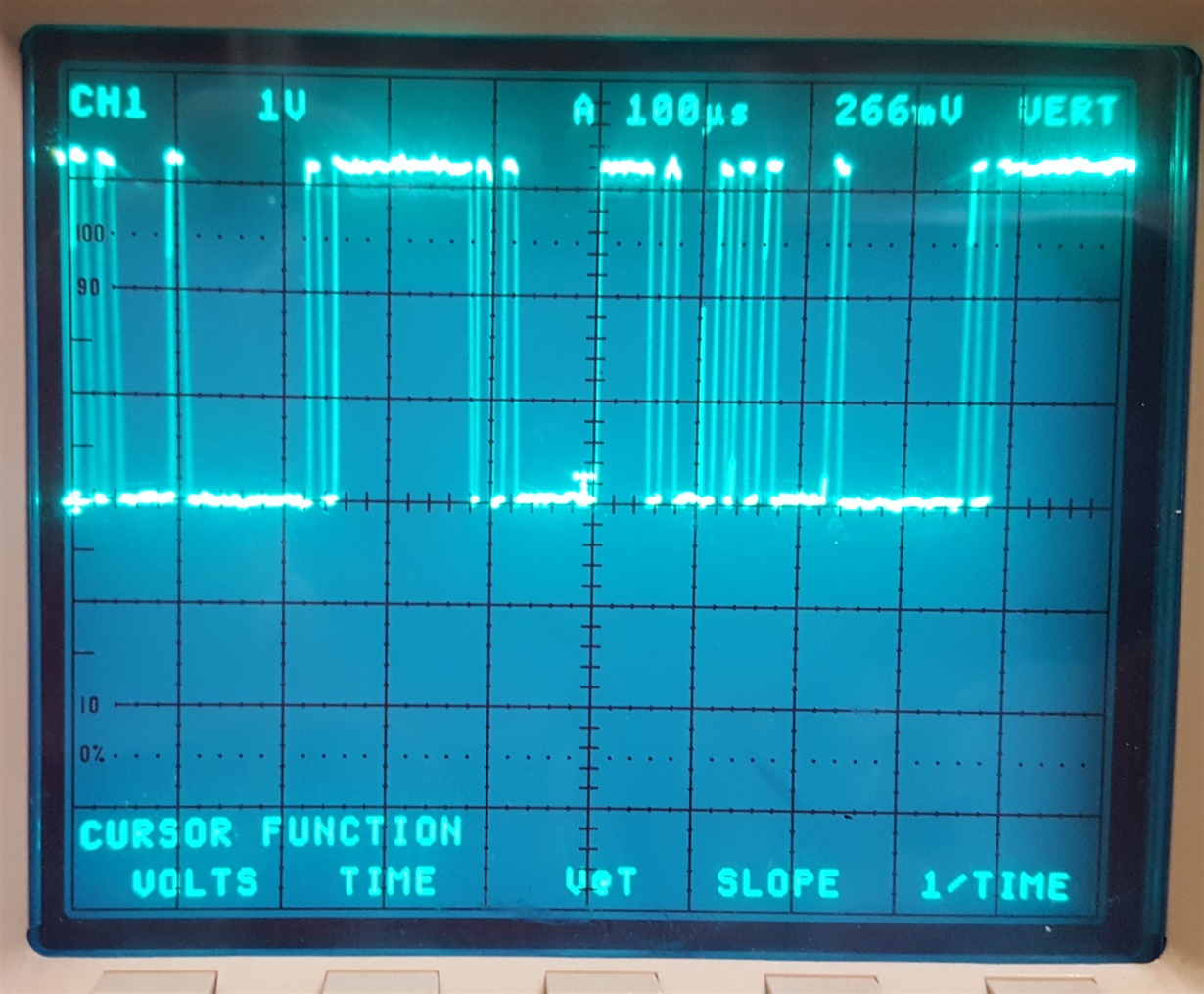
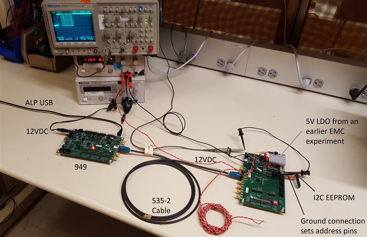
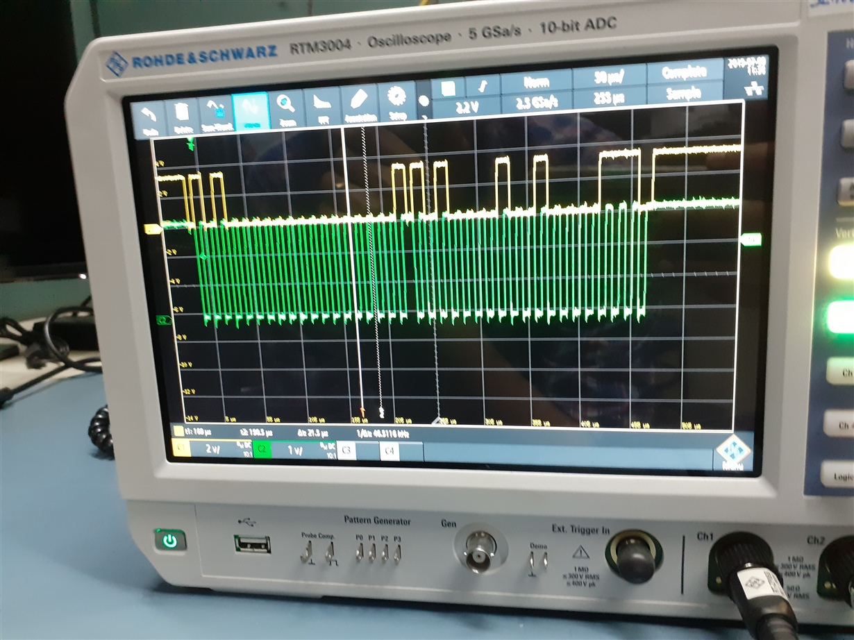
    • Power up the SERDES pair with a scope probe on the 948 SCL,SDA, and system power.  Trigger on the rising edge of system power.  If the EEPROM matches the EDID address in the 949 and the 948 sees the EEPROM on the I2C bus, the EDID transfer will look like the image below.  Note that the waveform is compressed and there is some aliasing; close-up images follow.
    • Close-up of I2C clock
    • Close-up of I2C data
    • If the I2C activity is very short (a byte or two) then the 948 did not see the EEPROM or the 949 was not configured correctly.
    • Check these 949 register bits and fix MODE_SEL0 and MODE_SEL1 if they don't match
        • 0x54 bit 7 = 0 Allows internal bridge control to function
        • 0x54 bit 5 = 0 Remote EDID load enabled when low
        • 0x5B bit 7 = 0 This is the setting for STP cable.  If you use coax, it should be 1.
        • 0x4F bit 0 = 0 Enables EDID access via DDC/I2C when set low.  I've filed a ticket to get the datasheet clarified.

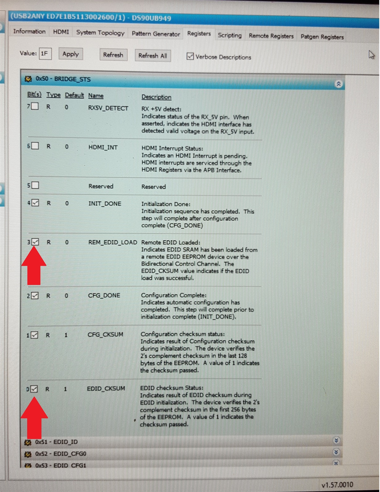
    • If the following bits are set, then the EDID is available in the 949 SRAM.  These bits were set in my setup:
    • 0x50 bit 3 = 1 Remote EDID loaded to SRAM
    • 0x50 bit 0 = 1 EDID transfer checksum passed

    I powered down, removed the EEPROM and then powered up to observe a failed EDID load.

    • Very short clock burst at the 948 I2C upon system power-up
    • 0x50 bit 3 = 0 indicating no remote EDID transfer

    Please follow this sequence exactly.  If it does not work, have the following ready at the debug phone call:

    • Scope plots of 948 I2C clk/data and system power at power-up
    • 949/948 register dump
    • Scope plots of MODE_SEL0 and MODE_SEL1 at power-up and voltage measurements of each after they stabilize.

    Mike

  • Hello Mike,

    Can you please send us a picture of working setup?

    Because in our case, 0x54(5) is 1 and 0x50(3) is 0 even after setting MODE_SEL switches.

    Thank you,

    Prathibha

  • Hi Prathibha,

    Here is my setup.

    If the MODE_SEL0 and MODE_SEL1 voltages don't match Table 7 and 8, please check the 1.8V rail voltage and adjust the resistors to get the correct MODE_SEL0 and MODE_SEL1 voltages.

    Mike

  • Hello Mike,

    When we set MODE_SEL1 to 4 or 3, we are reading 0x54 register as 0x28 where it is setting DIS_REM_EDID bit (0x54[5]).

    But when we set MODE_SEL1 to 2, we are able to read the register 0x54 as 0x08. This is not setting the DIS_REM_EDID bit but it will set 0x5B register to 0x20.

    In your setup, you are setting MODE_SEL1 to 2, this will enable the REM_EDID_LOAD option and also since you are not using coax cable, this mode selection is correct for you.

    Now the difference is, we are using Coax cable. So we have to go for MODE_SEL1 to 4 to keep the REM_EDID_LOAD and COAX options. But this is setting the DIS_REM_EDID bit of 0x54 register, and we are reading 0x50 as 0x97 which indicates EDID load is not successful.

    As you suggested to check the voltages, MODE_SEL1 voltage are matching with Table 8.

    Thank you,

    Prathibha

  • Hi Prathibha,

    When I set MODE_SEL1 to position 4, I got the settings you need at power-up.

    • 0x54(7)=0 internal bridge control enabled
    • 0x5B(7)=1 cable is coax
    • 0x54(5)=1 remote EDID load enabled (datasheet will be updated)

    I tested with MODE_SEL1 = 4 by powering up, capturing the EEPROM read on the 948 I2C, and verifying that 0x50=1.  So that should also be working in your setup.

    I did some experimenting and see that it is sensitive to slow power-up.  When I powered up by turning the power supply on with the wire harness attached, I did not always get an EEPROM read.  When I power up by hot-plugging the power wire into a supply that is already on and regulating it always reads the EEPROM.  Can you hot-plug power and capture the 948 I2C SCL?  If your 3.3V power rail comes up in 3mS or less, the EEPROM read should start about 30mS after power is applied.

    Mike

  • Hello Mike,

    We tested with hot plugging the power wires and still we do not see clock on I2C SCL line.

    Value in register 0x50 of serializer is 0x97, means 0x50 bit 3 (REM_EDID_LOAD) is still 0.

    Thank you,

    Prathibha

  • Hi Prathibha,

    Looks like MODE_SEL1 = 4 is the thing to solve.

    It is possible the position 4 resistor divider pair was mechanically damaged or are the wrong value.  Please replace them per the datasheet table.  Please add a 100pF cap in parallel to the lower resistor.  If there is noise, this will filter it and may help.  Have any changes been made to the 949 EVM?

    If that does not work, please try each of the MODE_SEL1 settings and record the bits below that you see at power-up before making any register changes.  If any position matches the bits below, please retest at that setting and we will sort out how the wrong mode is getting loaded.

    • 0x54(7)=0 internal bridge control enabled
    • 0x5B(7)=1 cable is coax
    • 0x54(5)=1 remote EDID load enabled (datasheet will be updated)

    Mike

  • Hello Mike,

    I tested with all the MODE_SEL1 settings, and every time I saw 949 register 0x50[3] as 0 only (0x50[3]=REM_EDID_LOAD).

    Can you please share your 949 register dump?

    Thank you,

    Prathibha

  • Hello Mike,

    Any updates?

  • Hello Mike,

    If we get 949 register dump from your working setup, we can check if any other register setting has gone different. 

    Can you please share the 949 register dump?

    Thank you,

    Prathibha

  • Hi Prathibha,

    Here is the register dump after a successful EDID read:

    [REGISTERS]
    Device = ALP Nano 1 - DS90UB949, Connector 1
    Comments = "REM_EDID_LOAD=1"
    Date = 07/08/2019
    Time = 17:52:48
    Reg = 0,0x0000,0x18
    Reg = 0,0x0001,0x00
    Reg = 0,0x0003,0xDA
    Reg = 0,0x0004,0x80
    Reg = 0,0x0005,0x00
    Reg = 0,0x0006,0x58
    Reg = 0,0x0007,0x00
    Reg = 0,0x0008,0x00
    Reg = 0,0x0009,0x00
    Reg = 0,0x000A,0x00
    Reg = 0,0x000B,0x00
    Reg = 0,0x000C,0x01
    Reg = 0,0x000D,0x20
    Reg = 0,0x000E,0x00
    Reg = 0,0x000F,0x00
    Reg = 0,0x0010,0x00
    Reg = 0,0x0011,0x00
    Reg = 0,0x0012,0x00
    Reg = 0,0x0013,0xB8
    Reg = 0,0x0014,0x00
    Reg = 0,0x0015,0x01
    Reg = 0,0x0016,0xFE
    Reg = 0,0x0017,0x1E
    Reg = 0,0x0018,0x7F
    Reg = 0,0x0019,0x7F
    Reg = 0,0x001A,0x01
    Reg = 0,0x001B,0x00
    Reg = 0,0x001C,0x00
    Reg = 0,0x001D,0x00
    Reg = 0,0x001E,0x01
    Reg = 0,0x001F,0xF6
    Reg = 0,0x0020,0x0B
    Reg = 0,0x0021,0x00
    Reg = 0,0x0022,0x25
    Reg = 0,0x0023,0x00
    Reg = 0,0x0024,0x00
    Reg = 0,0x0025,0x00
    Reg = 0,0x0026,0x00
    Reg = 0,0x0027,0x00
    Reg = 0,0x0028,0x01
    Reg = 0,0x0029,0x20
    Reg = 0,0x002A,0x20
    Reg = 0,0x002B,0xA0
    Reg = 0,0x002C,0x00
    Reg = 0,0x0030,0x00
    Reg = 0,0x0031,0x00
    Reg = 0,0x0032,0x00
    Reg = 0,0x0033,0x00
    Reg = 0,0x0034,0x00
    Reg = 0,0x0035,0x00
    Reg = 0,0x0036,0x00
    Reg = 0,0x0037,0x00
    Reg = 0,0x0038,0x00
    Reg = 0,0x0039,0x00
    Reg = 0,0x003A,0x00
    Reg = 0,0x003B,0x00
    Reg = 0,0x003C,0x00
    Reg = 0,0x003D,0x00
    Reg = 0,0x003E,0x00
    Reg = 0,0x003F,0x00
    Reg = 0,0x0040,0x14
    Reg = 0,0x0041,0x55
    Reg = 0,0x0042,0x00
    Reg = 0,0x0043,0x00
    Reg = 0,0x0044,0x80
    Reg = 0,0x0045,0x00
    Reg = 0,0x0046,0x00
    Reg = 0,0x0047,0x00
    Reg = 0,0x0048,0x00
    Reg = 0,0x0049,0x00
    Reg = 0,0x004A,0x00
    Reg = 0,0x004B,0x00
    Reg = 0,0x004C,0x00
    Reg = 0,0x004D,0x00
    Reg = 0,0x004E,0x00
    Reg = 0,0x004F,0x00
    Reg = 0,0x0050,0x1F
    Reg = 0,0x0051,0xA1
    Reg = 0,0x0052,0x1E
    Reg = 0,0x0053,0x00
    Reg = 0,0x0054,0x08
    Reg = 0,0x0055,0x0C
    Reg = 0,0x0056,0x00
    Reg = 0,0x0057,0x00
    Reg = 0,0x0058,0x00
    Reg = 0,0x0059,0x00
    Reg = 0,0x005A,0x92
    Reg = 0,0x005B,0xA0
    Reg = 0,0x005C,0x02
    Reg = 0,0x005D,0x06
    Reg = 0,0x005E,0x44
    Reg = 0,0x005F,0x00
    Reg = 0,0x0060,0x22
    Reg = 0,0x0061,0x02
    Reg = 0,0x0062,0x00
    Reg = 0,0x0064,0x10
    Reg = 0,0x0065,0x00
    Reg = 0,0x0066,0x00
    Reg = 0,0x0067,0x00
    Reg = 0,0x0068,0x00
    Reg = 0,0x0069,0x00
    Reg = 0,0x006A,0x00
    Reg = 0,0x006B,0x00
    Reg = 0,0x006C,0x00
    Reg = 0,0x0070,0x00
    Reg = 0,0x0071,0x00
    Reg = 0,0x0072,0x00
    Reg = 0,0x0073,0x00
    Reg = 0,0x0074,0x00
    Reg = 0,0x0075,0x00
    Reg = 0,0x0076,0x00
    Reg = 0,0x0077,0x00
    Reg = 0,0x0078,0x00
    Reg = 0,0x0079,0x00
    Reg = 0,0x007A,0x00
    Reg = 0,0x007B,0x00
    Reg = 0,0x007C,0x00
    Reg = 0,0x007D,0x00
    Reg = 0,0x0080,0x00
    Reg = 0,0x0081,0x00
    Reg = 0,0x0082,0x00
    Reg = 0,0x0083,0x00
    Reg = 0,0x0084,0x00
    Reg = 0,0x0090,0x00
    Reg = 0,0x0091,0x00
    Reg = 0,0x0092,0x00
    Reg = 0,0x0093,0x00
    Reg = 0,0x0094,0x00
    Reg = 0,0x0098,0x00
    Reg = 0,0x0099,0x00
    Reg = 0,0x009A,0x00
    Reg = 0,0x009B,0x00
    Reg = 0,0x009C,0x00
    Reg = 0,0x009D,0x00
    Reg = 0,0x009E,0x00
    Reg = 0,0x009F,0x00
    Reg = 0,0x00A0,0x00
    Reg = 0,0x00A1,0x00
    Reg = 0,0x00A2,0x00
    Reg = 0,0x00A3,0x00
    Reg = 0,0x00C0,0x00
    Reg = 0,0x00C1,0x00
    Reg = 0,0x00C2,0xA8
    Reg = 0,0x00C3,0x00
    Reg = 0,0x00C4,0x68
    Reg = 0,0x00C5,0x00
    Reg = 0,0x00C6,0x00
    Reg = 0,0x00C7,0xC0
    Reg = 0,0x00C8,0x40
    Reg = 0,0x00C9,0x00
    Reg = 0,0x00CA,0x00
    Reg = 0,0x00CB,0x00
    Reg = 0,0x00CC,0x00
    Reg = 0,0x00CE,0xFF
    Reg = 0,0x00D0,0x02
    Reg = 0,0x00D1,0xA1
    Reg = 0,0x00D2,0xFF
    Reg = 0,0x00D3,0x6F
    Reg = 0,0x00E0,0x00
    Reg = 0,0x00E1,0x00
    Reg = 0,0x00E2,0xA8
    Reg = 0,0x00E3,0x00
    Reg = 0,0x00E4,0x68
    Reg = 0,0x00E5,0x08
    Reg = 0,0x00E6,0x00
    Reg = 0,0x00E7,0x00
    Reg = 0,0x00F0,0x5F
    Reg = 0,0x00F1,0x55
    Reg = 0,0x00F2,0x42
    Reg = 0,0x00F3,0x39
    Reg = 0,0x00F4,0x34
    Reg = 0,0x00F5,0x39
    Reg = 0,0x00F6,0x00
    Reg = 0,0x00F8,0x00
    Reg = 0,0x00F9,0x00

  • Hello Mike,
    Thank you for sharing register dump.
    Now we are excluding SD820 and working only with serializer and deserializer. We don't have any driver control for serializer and deserializer from SD820 processor. Below is our test procedure,

    1. Connect EEPROM on deserializer
    2. Connect serializer and deserializer using coax cable on DOUT0 port
    3. Set MODE_SEL0=1 and MODE_SEL1=4 of serializer
    4. Power on both the serializer and deserializer by 12V
    5. Press PDB switch on serializer
    If we are only powering on then we see value in the register 0x54 as 0x28 but when we press PDB switch, we see 0x54 as 0x08.
    And we probed i2c lines at EEPROM when we press PDB switch. We saw some toggling on the line. Please find the picture attached.
    But still 0x50 register of serializer is 0x17(REM_EDID_LOAD=0), which is indicating edid has not loaded.
    And we see some CRC errors in the register 0x0A and 0x0C of serializer when we press PDB switch. 
    Thank you,
    Prathibha
  • Hi Prathibha,

    Good to see that you now have I2C activity on the deserializer to EEPROM I2C bus.

    When you power up but do not press the PDB, is the serializer RAM properly loaded with the EDID data?  Is REM_EDID_LOAD=1?

    I have copied a colleague with strong I2C background and will discuss with him this afternoon.

    Mike

  • Hello Mike,

    When we power up but do not press the PDB, the REM_EDID_LOAD=0. Serializer is not loaded with the remote EDID.

    Below is our test procedure. Please let us know other than pressing PDB, Are we missing anything?

    1. Mode select setting on serializer, MODE_SEL0=1 and MODE_SEL1=4

    2. Connecting an EEPROM programmed with the EDID at deserializer

    3. Connect serializer and deserializer using Coax cable at port0(DOUT0)

    4. Power on both serializer and deserializer with 12V

    5. After this we are checking the register values of serializer using Analog LaunchPAD

    And we get REM_EDID_LOAD=0(0x50=0x17) and DIS_REM_EDID=1(0x54=0x28) at this time.

    6. Press PDB switch and check for the register dump

    And we get REM_EDID_LOAD=0(0x50=0x17) and DIS_REM_EDID=0(0x54=0x08) at this time.

    Please let us know if we are missing anything. 

    And, Do you have any idea why are we getting CRC errors after pressing PDB switch?

    Thank you,

    Prathibha

  • Hello Mike,

    Any updates? And, Are we missing anything in the test procedure?

    Thank you,

    Prathibha

  • Hi Prathibha,

    Your procedure looks ok.  After step 5 is complete, I expect the EDID to be available in the 949 RAM.  Is it not there?

    When you press PDB on the 949 there may be some back channel errors because it reinitializes potentially in the middle of a 948 back channel transmission.  In that case there should be some initial errors, but they should not accumulate after that.  Is that what you are seeing?

    Mike

  • Additional item, I am using the PCF8582C EEPROM.

  • Hi Prathibha,

    In your register dump address 0x13 contains 0xA8 and in my register dump it is 0xB8.

    That means you are in MODE_SEL1 = 3, so REM_EDID_LOAD=0 and the system will not attempt to get the remote EEPROM EDID.

    My register 0x13 contains 0xB8, so MODE_SEL1 = 4 and REM_EDID_LOAD=1 and remote EEPROM EDID is loading.

    Please fix your MODE_SEL1 resistor ratio.

    Are you using a TI EVM or your internal design on the 949 side?

    Mike

  • Hi Prathibha,

    Your TI FAE shared your latest register dump in an email.  MODE_SEL1 needs to be correct before you can make progress.

    Please make sure you are getting 0.792V on MODE_SEL1 pin and see MODE 4 in the register.

    If you are, please capture the supply rails, PDB, and MODE_SEL1 on a scope.

    Mike

  • Hello Mike,

    The register 0x13 has 0xA8 before pressing PDB switch and it is 0xB8 after pressing PDB switch.

    We probed MODE_SEL1 switch at mode 4 pin and we are getting around 0.79V before and after pressing PDB switch.

    And below are the steps to generate EDID data and writing it to EEPROM,

    1. Use "AW EDID Editor" tool to generate the EDID data according to our display specifications

    2. Take Hexadecimal values of that EDID data

    3. Use echo command to write the data to EEPROM as a string, Ex:- 'echo "Hex value of the edid data" > /sys/bus/i2c/devices/8-0050/eeprom'

    Is this procedure to write the EDID data to EEPROM is correct? or Can we know what method are you using to write the EDID data to EEPROM?

    Thank you,

    Prathibha

  • Hello Mike,

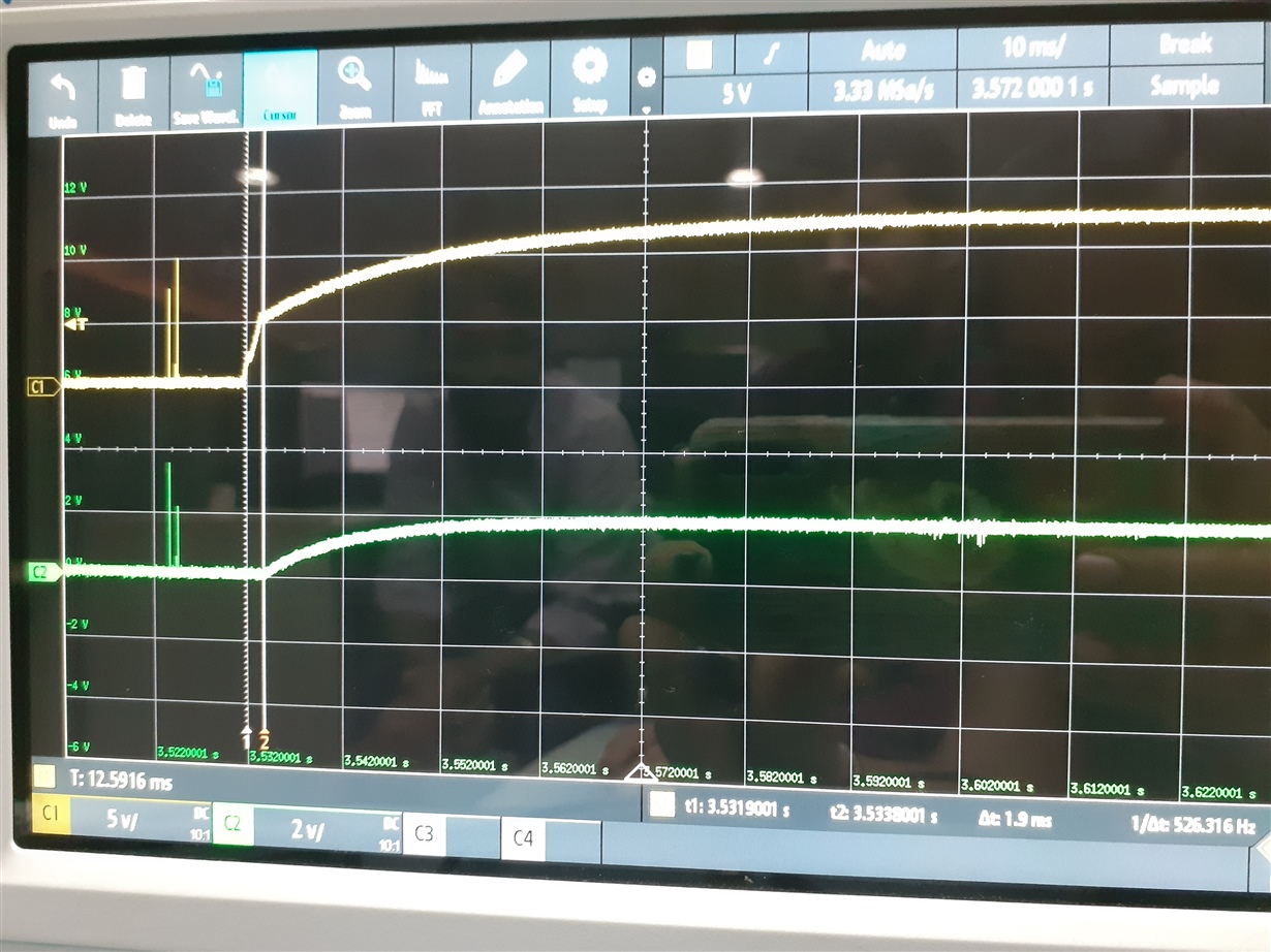
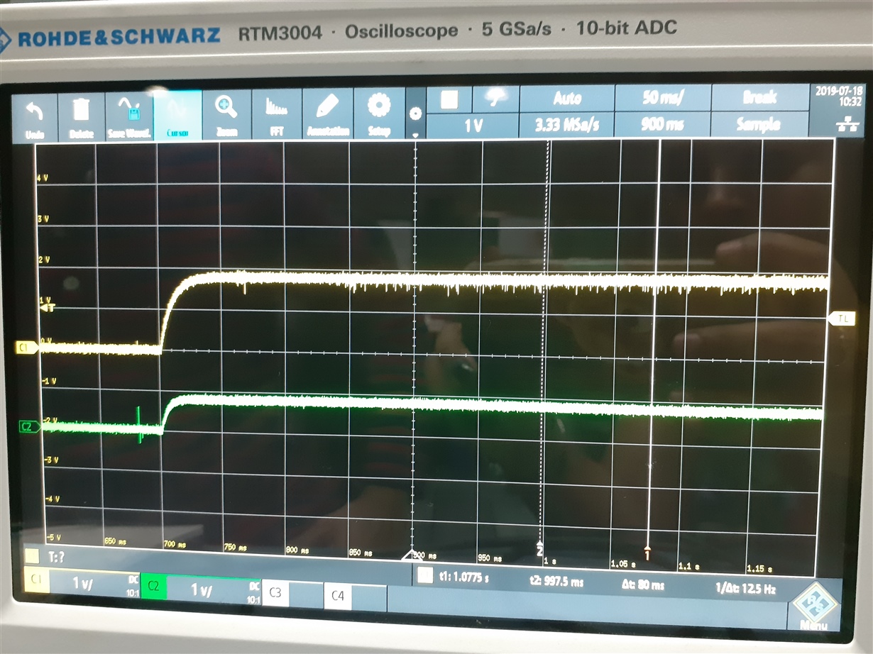
    Below are the waveforms which we capture.

    1. Ch1-Supply and Ch2-PDB

    2. Ch1-PDB and Ch2-MODE4 pin and MODE_SEL1 switch

    Thank you,

    Prathibha 

  • Hello Mike,

    Is there any update on procedure to write EDID data to EEPROM?

    The method whatever we are following, Is that correct?

    Thank you,

    Prathibha

  • Hi Prathibha,

    I don't see anything wrong with the procedure, just with MODE_SEL1 coming up wrong then correct after PDB. 

    This suggests that the MODE_SEL1 pin is ramping up at a slow rate.  Is there a capacitor on MODE_SEL1?  If yes, the RC delay on the pin would explain this behavior.  Please check for that.

    Can you try to PDB both 948/949 at the exact same time?

    Mike

  • Since we have been having emails and phone calls on this topic directly I will close this ticket and update later once we have resolved the issue 

    Best Regards,

    Casey