


Other Parts Discussed in Thread: DS125DF1610
Hi expert:
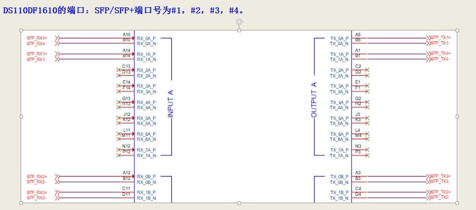
My customer use DS110DF1610 for conversion card. The schematic diagram of our product is as follows:
Because some cards can be locked, but some cards can not be locked. Later the cards were modified to not use cross point and not to use the manually set rate, the result is the same as before.
Attached is the chip initialization program, the debugging information of cards that cannot be locked and debugging information of the cards that can be locked .
Ds110DF1610.c
void ds110df1610_init(unsigned char card_type, unsigned char sw, unsigned char work_mode)
{
unsigned char regvalue = 0, i = 0;
unsigned char low, high;
unsigned int val;
rt_thread_delay(200);// wait chip ready, old is 50
i2c_lock();
regvalue = 0x00;
i2c_write_ds280df810(0xff, ®value);//select shared
i2c_read_ds280df810(0x01,®value);//high 3bit device verion, low 5 bit device id
rt_kprintf("dev info = 0x%02x (high 3bit device version, low 5 bit device id)\r\n", regvalue);
i2c_read_ds280df810(0xfe,®value);
rt_kprintf("vendor id = 0x%02x (expect 0x03)\r\n",regvalue);
regvalue = 0x00;
i2c_write_ds280df810(0x02, ®value);//Sets the REFCLK input frequency as 25M
i2c_write_ds280df810_withmask(0x0B, 0x10, 0x10);//single-ended input
i2c_write_ds280df810_withmask(0x05, 0x08, 0x0f);//sets max number of channels that can lock at any given time.
//i2c_write_ds280df810_withmask(0xff, 0x00, 0x03);//select shared
//i2c_write_ds280df810_withmask(0x02, 0x00, 0x60);//Sets the REFCLK input frequency as 25M
//i2c_write_ds280df810_withmask(0x0B, 0x10, 0x10);//single-ended input
i2c_write_ds280df810_withmask(0xff, 0x01, 0x03);//select channel
regvalue = 0;
i2c_write_ds280df810(0xfd, ®value);
rt_kprintf("rate = 0x%02x;work_mode = 0x%02x\r\n",sw,work_mode);
for(i = 0; i < 4; i++){
regvalue = (1<<i);
i2c_write_ds280df810(0xfc, ®value);
i2c_write_ds280df810_withmask(0x0, 0x04, 0x04);//reset channel register to power-on default values
i2c_write_ds280df810_withmask(0xa, 0x0c, 0x0c);//assert CDR reset
//TBD
//set rate, more rate programming, refer to page 68, the section 7.2.2 Data Rate Selection (Manual Programming)
i2c_write_ds280df810_withmask(0x2f, 0xc0, 0xf0);//set rate as 10.3125Gbps
//adapt mode
i2c_write_ds280df810_withmask(0x31, 0x60, 0x60);//adapt mode1:only CTLE
//i2c_write_ds280df810_withmask(0x31, 0x0, 0x60);//no adapt
//i2c_write_ds280df810_withmask(0x31, 0x40, 0x60);//adapt mode2
//i2c_write_ds280df810_withmask(0x31, 0x60, 0x60);//adapt mode3
//i2c_write_ds280df810_withmask(0x1e, 0x08, 0x0a);//disable dfe ?
i2c_write_ds280df810_withmask(0x1e, 0x08, 0x08);//enable dfe ?
i2c_write_ds280df810_withmask(0x3d, 0x00, 0x80);//enable fir ?
i2c_write_ds280df810_withmask(0x3d, 0x0, 0x40);//main-cursor tap sign to positive
i2c_write_ds280df810_withmask(0x3f, 0x40, 0x40);//post-cursor tap sign to negative
i2c_write_ds280df810_withmask(0x3e, 0x40, 0x40);//pre-cursor tap sign to negative
i2c_write_ds280df810_withmask(0x3d, 0x0c, 0x3f);//main-cursor tap magnitude
i2c_write_ds280df810_withmask(0x3f, 0x0, 0x3f);//post-cursor tap magnitude
i2c_write_ds280df810_withmask(0x3e, 0x0, 0x3f);//pre-cursor tap magnitude
i2c_write_ds280df810_withmask(0x0a, 0x00, 0x0c);//release CDR reset
}
for(i = 4; i < 8; i++){
regvalue = (1<<i);
i2c_write_ds280df810(0xfc, ®value);
i2c_write_ds280df810_withmask(0x15, 0x18, 0xff);//Power down the driver
i2c_write_ds280df810_withmask(0x14, 0x44, 0xff);//Force signal detect status to 0
i2c_write_ds280df810_withmask(0x13, 0xf0, 0xff);//Power down signal detect block
}
regvalue = 0;
i2c_write_ds280df810(0xfc, ®value);
for(i = 0; i < 8; i++){
regvalue = (1<<i);
i2c_write_ds280df810(0xfd, ®value);
i2c_write_ds280df810_withmask(0x15, 0x18, 0xff);//Power down the driver
i2c_write_ds280df810_withmask(0x14, 0x44, 0xff);//Force signal detect status to 0
i2c_write_ds280df810_withmask(0x13, 0xf0, 0xff);//Power down signal detect block
}
i2c_unlock();
//set_board_rate(4,sw);
}
debug information of card that can be locked.txt
�����߿�Ҳ������SFP1(RX0A)��SFP4��RX1A�����������ĸ�ͨ���ĵ�����Ϣ��
finsh>>show_cdr()
Horizontal and Vertical Eye:HEO_UI=val/32,VEO_mV=val*3.125
CH 0:
HEO_UI=21 ,VEO_mV=62
CTLE boost value=2
Status reg[0x78]=0x30[5:SD,4:LCK]
ch reg[0x31]=0x60, bit6:5-adapt mode
adapt3:CTLE until lock,then dfe,the eq
ch reg[0x1e]=0xe9, bit3-DFE switch
DFE disable
Main:0xc[6:Sign,5-0:mag]
Post:0xc0[6:Sign,5-0:mag]
Pre:0x40[6:Sign,5-0:mag]
CH 1:
HEO_UI=0 ,VEO_mV=0
CTLE boost value=165
Status reg[0x78]=0x0[5:SD,4:LCK]
ch reg[0x31]=0x60, bit6:5-adapt mode
adapt3:CTLE until lock,then dfe,the eq
ch reg[0x1e]=0xe9, bit3-DFE switch
DFE disable
Main:0xc[6:Sign,5-0:mag]
Post:0xc0[6:Sign,5-0:mag]
Pre:0x40[6:Sign,5-0:mag]
CH 2:
HEO_UI=25 ,VEO_mV=70
CTLE boost value=0
Status reg[0x78]=0x30[5:SD,4:LCK]
ch reg[0x31]=0x60, bit6:5-adapt mode
adapt3:CTLE until lock,then dfe,the eq
ch reg[0x1e]=0xe9, bit3-DFE switch
DFE disable
Main:0xc[6:Sign,5-0:mag]
Post:0xc0[6:Sign,5-0:mag]
Pre:0x40[6:Sign,5-0:mag]
CH 3:
HEO_UI=0 ,VEO_mV=0
CTLE boost value=165
Status reg[0x78]=0x0[5:SD,4:LCK]
ch reg[0x31]=0x60, bit6:5-adapt mode
adapt3:CTLE until lock,then dfe,the eq
ch reg[0x1e]=0xe9, bit3-DFE switch
DFE disable
Main:0xc[6:Sign,5-0:mag]
Post:0xc0[6:Sign,5-0:mag]
Pre:0x40[6:Sign,5-0:mag]
        0, 0x00000000
debug information of card that can not be locked.txt
�����߿�������SFP1(RX0A)��SFP4��RX1A�����������ĸ�ͨ���ĵ�����Ϣ��
finsh>>show_cdr()
Horizontal and Vertical Eye:HEO_UI=val/32,VEO_mV=val*3.125
CH 0:
HEO_UI=0 ,VEO_mV=0
CTLE boost value=165
Status reg[0x78]=0x20[5:SD,4:LCK]
ch reg[0x31]=0x60, bit6:5-adapt mode
adapt3:CTLE until lock,then dfe,the eq
ch reg[0x1e]=0xe9, bit3-DFE switch
DFE disable
Main:0xc[6:Sign,5-0:mag]
Post:0xc0[6:Sign,5-0:mag]
Pre:0x40[6:Sign,5-0:mag]
CH 1:
HEO_UI=0 ,VEO_mV=0
CTLE boost value=165
Status reg[0x78]=0x0[5:SD,4:LCK]
ch reg[0x31]=0x60, bit6:5-adapt mode
adapt3:CTLE until lock,then dfe,the eq
ch reg[0x1e]=0xe9, bit3-DFE switch
DFE disable
Main:0xc[6:Sign,5-0:mag]
Post:0xc0[6:Sign,5-0:mag]
Pre:0x40[6:Sign,5-0:mag]
CH 2:
HEO_UI=0 ,VEO_mV=0
CTLE boost value=165
Status reg[0x78]=0x20[5:SD,4:LCK]
ch reg[0x31]=0x60, bit6:5-adapt mode
adapt3:CTLE until lock,then dfe,the eq
ch reg[0x1e]=0xe9, bit3-DFE switch
DFE disable
Main:0xc[6:Sign,5-0:mag]
Post:0xc0[6:Sign,5-0:mag]
Pre:0x40[6:Sign,5-0:mag]
CH 3:
HEO_UI=0 ,VEO_mV=0
CTLE boost value=165
Status reg[0x78]=0x0[5:SD,4:LCK]
ch reg[0x31]=0x60, bit6:5-adapt mode
adapt3:CTLE until lock,then dfe,the eq
ch reg[0x1e]=0xe9, bit3-DFE switch
DFE disable
Main:0xc[6:Sign,5-0:mag]
Post:0xc0[6:Sign,5-0:mag]
Pre:0x40[6:Sign,5-0:mag]
        0, 0x00000000
Please help to analyze what causes the failure of locking and explain the process of chip locking.Any advice will be apprreciated.
Best regards


